-
Description
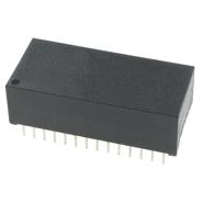
This document contains the specifications for the Intel® Advanced+ Boot Block Flash Memory (C3) Stacked Chip Scale Package (SCSP) device. C3 SCSP memory solutions are offered in the following combinations:
• 32-Mbit flash + 8-Mbit SRAM
• 32-Mbit flash + 4-Mbit SRAM
• 16-Mbit flash + 4-Mbit SRAM
• 16-Mbit flash memory + 2-Mbit SRAMThe C3 SCSP device combines flash memory and SRAM into a single package, which provides secure low-voltage memory solutions for portable applications.
The flash memory provides the following features:
• Enhanced security.
• Instant locking/unlocking of any flash block with zero-latency
• A 128-bit protection register that enables unique device identification,
to meet the needs ofnext generation portable applications.
• Improved 12 V production programming for increased factory throughput.Specifications and features
■ Flash Memory Plus SRAM
—Reduces Memory Board Space
Required, Simplifying PCB Design
Complexity
■ SCSP Technology
—Smallest Memory Subsystem Footprint
—Area : 8 x 10 mm for 16 Mbit (0.13 µm)
Flash + 2 Mbit or 4 Mbit SRAM
—Area : 8 x 12 mm for 32 Mbit (0.13 µm)
Flash + 4 Mbit or 8 Mbit SRAM
—Height : 1.20 mm for 16 Mbit (0.13 µm)
Flash + 2 Mbit or 4 Mbit SRAM, and 32
Mbit (0.13um) Flash + 8 Mbit SRAM
—Height : 1.40 mm for 32 Mbit (0.13 µm)
Flash + 4 Mbit SRAM
—This Family also includes 0.25 µm, 0.18
µm, and 0.13 µm technologies
■ Advanced SRAM Technology
—70 ns Access Time
—Low Power Operation
—Low Voltage Data Retention Mode
■ Intel® Flash Data Integrator (FDI) Software
—Real-Time Data Storage and Code
Execution in the Same Memory Device
—Full Flash File Manager Capability
■ Advanced+ Boot Block Flash Memory
—70 ns Access Time
—Instant, Individual Block Locking
—128 bit Protection Register
—12 V Production Programming
—Fast Program and Erase Suspend
—Extended Temperature –25 °C to +85 °C
■ Blocking Architecture
—Block Sizes for Code + Data Storage
—4-Kword Parameter Blocks
—64-Kbyte Main Blocks
—100,000 Erase Cycles per Block
■ Low Power Operation
—Asynchronous Read Current: 9 mA (Flash)
—Standby Current: 7 µA (Flash)
—Automatic Power Saving Mode
■ Flash Technologies
—0.25 µm ETOX™ VI, 0.18 µm ETOX™
VII and 0.13 µm ETOX™ VIII Flash
TechnologiesApplication Scenarios
The Intel® Advanced+ Boot Block Flash Memory (C3) Stacked Chip Scale Package (SCSP) device is designed for portable applications that require secure low-voltage memory solutions. It can be used in various electronic devices such as smartphones, tablets, portable gaming consoles, and wearable devices.
Comparison
Advantages- Combines flash memory and SRAM into a single package, reducing memory board space and simplifying PCB design complexity.
- Flash memory provides enhanced security features, instant locking/unlocking of any flash block with zero-latency, and a 128-bit protection register for unique device identification.
- Improved 12 V production programming for increased factory throughput.
- Advanced SRAM technology with low power operation and low voltage data retention mode.
- Intel® Flash Data Integrator (FDI) Software enables real-time data storage and code execution in the same memory device.
- Advanced+ Boot Block Flash Memory with individual block locking, fast program and erase suspend, and extended temperature range (-25 °C to +85 °C).
Disadvantages- Limited available combinations of flash memory and SRAM capacities (32-Mbit flash + 8-Mbit SRAM, 32-Mbit flash + 4-Mbit SRAM, 16-Mbit flash + 4-Mbit SRAM, 16-Mbit flash + 2-Mbit SRAM).
-
Similar parts: 9920 , Click to view
-
Datasheet
-
Shopping guide
Delivery period:
- - Will ship out in 2-3 days
- - DHL Express: 3-7 business days
- - DHL eCommerce: 12-22 business days
- - FedEx International Priority: 3-7 business days
- - EMS: 10-15 business days
Shipping fee:
- - Automatic Email notification (above 5 times)
- - View in your order page
Shipping option:
DHL, FedEx, EMS, SF Express, and Registered Air MailShipping tracking:
- - Automatic Email notification (above 5 times)
- - View in your order page
How to Buy:
- - In-stock, Add to cart > Check out > Submit order > Complete payment >Delivery.
- - Inquiry, Add to inquiry sheet/Submit bom/inquire file/Send email us > Quote > Place order > Complete payment >Delivery.
- View more
Payment:
- - Paypal,Credit Card includes Visa, Master, American Express.
- - Wire transfer, include Local bank transfer.
- - Western Union.
- View more
-
Popular parts of the same kind
- Datasheet: Download RD38F2020W0YBQ0
- Chipdatas Part: CD93-RD38F2020W0YBQ0
- Warehouse: China, Hong Kong
- Dispatch: Within 24 hours
- Free Shipping: Yes
- Prority Shipping: Yes, 3-5 days
- Last Updated: 2024/10/01 12:40 +0800
-
- Full Refund if you don't receive your order
- Full or Partial Refund , If the item is not as described
-
 M25P80-VMN6TP - Brand New Micron Technology Inc. MemorySOP-8
 -
 MT48LC8M16A2P-6A:L - Brand New Micron Technology Inc. MemoryTSOP-54
 -
 M29W040B-90K1 - Brand New STMicroelectronics MemoryPLCC
 -
 W25Q64BVSFIG - Brand New Winbond Electronics MemorySOP-16
 -
 PC28F128J3D-75 - Brand New INTEI MemoryBGA
 -
 DS1225Y - Brand New Texas Instruments MemoryMOUDLE
 -
 DS2431Q+T&R - Brand New Maxim Integrated Memory6-WDFN Exposed Pad
 -
 IS61LV25616AL-10TLI - Brand New ISSI Memory44-TSOP 0.400", 10.16mm Width
 -
 AT93C66B-XHM-T - Brand New Intel / Altera Memory8-TSSOP 0.173", 4.40mm Width
 -
 AT24C128C-XHM-T - Brand New Intel / Altera MemoryTSSOP
-
The fee is charged according to the rule of PayPal.
-
The fee is charged according to the rule of PayPal.
-
Western Union charge US$0.00 banking fee.
-
We recommend to use bank transfer for large orders to save on handling fees.
-
DHL(www.dhl.com)
$40 limited time offer. -
UPS(www.ups.com)
$40 limited time offer. -
FedEx(www.fedex.com)
$40 limited time offer. -
Registered Mail(www.singpost.com)
Free shipping without minimum order.
