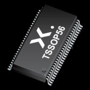
74LVT16500ADGG - Brand New NXP Semiconductors Universal Bus Function
-
Description
The 74LVT16500ADGG is a high-performance BiCMOS electronic component that belongs to the Universal Bus Function product category, designed for VCC operation at 3.3 V. It features 18-bit bidirectional bus interface, 3-state buffers, and TTL input and output switching levels. The component comes with input and output interface capability to systems at 5 V supply and bus-hold data inputs that eliminate the need for external pull-up resistors to hold unused inputs. Additionally, the 74LVT16500ADGG has live insertion/extraction permitted feature, power-up reset and 3-state, no bus current loading when output is tied to 5 V bus, negative edge-triggered clock inputs, and latch-up and ESD protections that exceed 500 mA and 2000 V, respectively.
Specifications and Features
- Product Category: Universal Bus Function
- Operating Voltage: 3.3 V
- Interface: 18-bit bidirectional bus interface, TTL input and output switching levels
- Output Capability: +64 mA and −32 mA
- Input and Output Interface Capability to Systems at 5 V Supply
- Bus-hold Data Inputs
- Live Insertion/Extraction Permitted
- Power-up Reset
- Power-up 3-state
- No Bus Current Loading When Output is Tied to 5 V Bus
- Negative Edge-triggered Clock Inputs
- Latch-up Protection: Exceeds 500 mA (JESD78)
- ESD Protection: Exceeds 2000 V (MIL STD 883 Method 3015), Exceeds 1000 V CDM (JESD22-C101-C)
Application Scenarios
The 74LVT16500ADGG can be used in various electronic systems that require high-performance bus interface and reliable operation. This component is ideal for applications that operate at 3.3 V and require interface capability to systems at 5 V supply.
Comparison
Advantages- 18-bit bidirectional bus interface
- TTL input and output switching levels
- Input and output interface capability to systems at 5 V supply
- Bus-hold data inputs eliminate the need for external pull-up resistors to hold unused inputs
- Live insertion/extraction permitted
- Power-up reset and 3-state
- No bus current loading when output is tied to 5 V bus
- Negative edge-triggered clock inputs
- Latch-up and ESD protections that exceed 500mA and 2000V
Disadvantages- May not be suitable for applications that require operation at voltages other than 3.3 V or 5 V
-
Similar parts: 211 , Click to view
-
Datasheet
-
Shopping guide
Delivery period:
- - Will ship out in 2-3 days
- - DHL Express: 3-7 business days
- - DHL eCommerce: 12-22 business days
- - FedEx International Priority: 3-7 business days
- - EMS: 10-15 business days
Shipping fee:
- - Automatic Email notification (above 5 times)
- - View in your order page
Shipping option:
DHL, FedEx, EMS, SF Express, and Registered Air MailShipping tracking:
- - Automatic Email notification (above 5 times)
- - View in your order page
How to Buy:
- - In-stock, Add to cart > Check out > Submit order > Complete payment >Delivery.
- - Inquiry, Add to inquiry sheet/Submit bom/inquire file/Send email us > Quote > Place order > Complete payment >Delivery.
- View more
Payment:
- - Paypal,Credit Card includes Visa, Master, American Express.
- - Wire transfer, include Local bank transfer.
- - Western Union.
- View more
-
Popular parts of the same kind
- Datasheet: Download 74LVT16500ADGG
- Chipdatas Part: CD86-74LVT16500ADGG
- Warehouse: China, Hong Kong
- Dispatch: Within 24 hours
- Free Shipping: Yes
- Prority Shipping: Yes, 3-5 days
- Last Updated: 2024/10/01 07:56 +0800
-
- Full Refund if you don't receive your order
- Full or Partial Refund , If the item is not as described
-
 ALVCH16901DGGR - Brand New Texas Instruments Universal Bus FunctionTSSOP-64
 -
 AVC16834 - Brand New Texas Instruments Universal Bus FunctionSOP
 -
 VCX16601MTD - Brand New onsemi Universal Bus FunctionTSSOP
 -
 74AVC16334ADGG - Brand New PHILIPS Universal Bus FunctionTSSOP
 -
 74ALVC16835DGG - Brand New PHI Universal Bus FunctionTSSOP-56
 -
 VCX16601 - Brand New onsemi Universal Bus FunctionTSSOP
 -
 SN74ALVC162334DGGR - Brand New Texas Instruments Universal Bus Function48-TFSOP 0.240", 6.10mm Width
 -
 SN74GTL1655DGGR - Brand New Texas Instruments Universal Bus Function64-TFSOP 0.240", 6.10mm Width
 -
 SN74ALVCH16269DGGR - Brand New Texas Instruments Universal Bus Function56-TFSOP 0.240", 6.10mm Width
 -
 SN74ALVTH16601GR - Brand New Texas Instruments Universal Bus Function56-TFSOP 0.240", 6.10mm Width
-
The fee is charged according to the rule of PayPal.
-
The fee is charged according to the rule of PayPal.
-
Western Union charge US$0.00 banking fee.
-
We recommend to use bank transfer for large orders to save on handling fees.
-
DHL(www.dhl.com)
$40 limited time offer. -
UPS(www.ups.com)
$40 limited time offer. -
FedEx(www.fedex.com)
$40 limited time offer. -
Registered Mail(www.singpost.com)
Free shipping without minimum order.
