SST49LF002A-33-4C-NHSST - Brand New SST IC Chips
-
Description
The SST49LF00xA flash memory devices are designed to be read-compatible with the Intel 82802 Firmware Hub (FWH) device for PC-BIOS application. It provides protection for the storage and update of code and data in addition to adding system design flexibility through five general purpose inputs. Two interface modes are supported by the SST49LF00xA: Firmware Hub (FWH) Interface Mode for In-System programming and Parallel Programming (PP) Mode for fast factory programming of PC-BIOS applications.
Specifications and features
• Firmware Hub for Intel 8xx Chipsets
• 2 Mbit, 3 Mbit, 4 Mbit, or 8 Mbit SuperFlash memory array for code/data storage
– SST49LF002A: 256K x8 (2 Mbit)
– SST49LF003A: 384K x8 (3 Mbit)
– SST49LF004A: 512K x8 (4 Mbit)
– SST49LF008A: 1024K x8 (8 Mbit)
• Flexible Erase Capability
– Uniform 4 KByte Sectors
– Uniform 16 KByte overlay blocks for SST49LF002A
– Uniform 64 KByte overlay blocks for SST49LF003A/004A/008A
– Top Boot Block protection
- 16 KByte for SST49LF002A
- 64 KByte for SST49LF003A/004A/008A
– Chip-Erase for PP Mode Only
• Single 3.0-3.6V Read and Write Operations
• Superior Reliability
– Endurance:100,000 Cycles (typical)
– Greater than 100 years Data Retention
• Low Power Consumption
– Active Read Current: 6 mA (typical)
– Standby Current: 10 µA (typical)
• Fast Sector-Erase/Byte-Program Operation
– Sector-Erase Time: 18 ms (typical)
– Block-Erase Time: 18 ms (typical)
– Chip-Erase Time: 70 ms (typical)
– Byte-Program Time: 14 µs (typical)
– Chip Rewrite Time:
SST49LF002A: 4 seconds (typical)
SST49LF003A: 6 seconds (typical)
SST49LF004A: 8 seconds (typical)
SST49LF008A: 15 seconds (typical)
– Single-pulse Program or Erase
– Internal timing generation
• Two Operational Modes
– Firmware Hub Interface (FWH) Mode for in-system operation
– Parallel Programming (PP) Mode for fast production programming
• Firmware Hub Hardware Interface Mode
– 5-signal communication interface supporting byte Read and Write
– 33 MHz clock frequency operation
– WP# and TBL# pins provide hardware write protect for entire chip and/or top Boot Block
– Block Locking Register for all blocks
– Standard SDP Command Set
– Data# Polling and Toggle Bit for End-of-Write detection
– 5 GPI pins for system design flexibility
– 4 ID pins for multi-chip selection
• Parallel Programming (PP) Mode
– 11-pin multiplexed address and 8-pin data I/O interface
– Supports fast In-System or PROM programming for manufacturing
• CMOS and PCI I/O Compatibility
• Packages Available
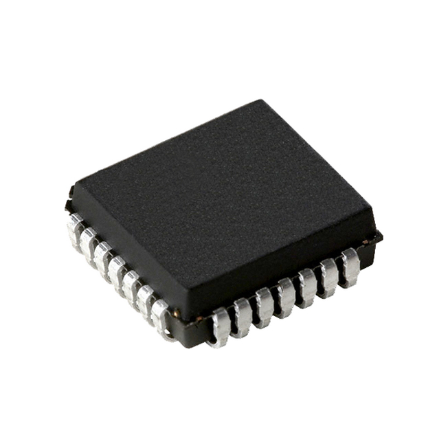
– 32-lead PLCC
– 32-lead TSOP (8mm x 14mm)Application Scenarios
Electronic products that require flash memory for code and data storage and update. Ideal for PC-BIOS applications and manufacturing programming.
Comparison
Advantages- Read-compatible with the Intel 82802 Firmware Hub (FWH) device
- Provides protection for the storage and update of code and data
- Offers system design flexibility through five general purpose inputs
- Supports two interface modes: Firmware Hub (FWH) Interface Mode and Parallel Programming (PP) Mode
- Flexible erase capability with uniform sectors and overlay blocks
- Low power consumption and superior reliability
- Fast sector-erase and byte-program operation
- Two operational modes for in-system programming and fast production programming
- Supports hardware write protect and block locking
- Supports CMOS and PCI I/O Compatibility
- Available in multiple package optionsDisadvantages- Limited memory capacity options
- May not be compatible with all electronic products and applications -
ähnliche Teile: 430483 , Klicke zum Zeigen
-
Datenblatt
-
Shopping guide
Delivery period:
- - Will ship out in 2-3 days
- - DHL Express: 3-7 business days
- - DHL eCommerce: 12-22 business days
- - FedEx International Priority: 3-7 business days
- - EMS: 10-15 business days
Shipping fee:
- - Automatic Email notification (above 5 times)
- - View in your order page
Shipping option:
DHL, FedEx, EMS, SF Express, and Registered Air MailShipping tracking:
- - Automatic Email notification (above 5 times)
- - View in your order page
How to Buy:
- - In-stock, Add to cart > Check out > Submit order > Complete payment >Delivery.
- - Inquiry, Add to inquiry sheet/Submit bom/inquire file/Send email us > Quote > Place order > Complete payment >Delivery.
- View more
Payment:
- - Paypal,Credit Card includes Visa, Master, American Express.
- - Wire transfer, include Local bank transfer.
- - Western Union.
- View more
-
Beliebte Teile der gleichen Art
- Datasheet: Download SST49LF002A-33-4C-NHSST
- Chipdaten Teil: CD94-SST49LF002A-33-4C-NHSST
- Lagerhaus: China, Hongkong
- Versenden: Innerhalb von 24 Stunden
- Kostenloser Versand: Yes
- Bevorzugter Versand: Yes, 3-5 days
- Letzte Aktualisierung: 2024/10/01 00:52 +0800
-
- Vollständige Rückerstattung, wenn Sie Ihre Bestellung nicht erhalten
- Vollständige oder teilweise Rückerstattung, wenn der Artikel nicht der Beschreibung entspricht
-
 E-STLC2500CTR - Brand New STMicroelectronics IC ChipsWFBGA
 -
 CY7C68053A-56BA - Brand New Cypress Semiconductor IC ChipsBGA
 -
 AR8035-AL1A-R - Brand New QCA IC ChipsBGA
 -
 BL1117-ADC - Brand New Belling IC ChipsSOT-223
 -
 HM628512BLFP-7 - Brand New Nexperia IC ChipsSOP-32
 -
 BCM5325FKQMG - Brand New Broadcom IC ChipsQFP
 -
 D431000AGW-70LL - Brand New NEC IC ChipsSOP
 -
 HT46R003B - Brand New HOLTEK IC ChipsSOP-16
 -
 BCM2045KWBG - Brand New Broadcom IC ChipsBGA
 -
 H26M52103FMR - Brand New Skhynix IC ChipsBGA
-
Die Gebühr wird gemäß der PayPal-Regel erhoben.
-
Die Gebühr wird gemäß der PayPal-Regel erhoben.
-
Western Union erhebt eine Bankgebühr von 0,00 US-Dollar.
-
Wir empfehlen, bei größeren Bestellungen die Banküberweisung zu nutzen, um Bearbeitungsgebühren zu sparen.
-
DHL(www.dhl.com)
Zeitlich begrenztes Angebot im Wert von 40 $. -
UPS(www.ups.com)
Zeitlich begrenztes Angebot im Wert von 40 $. -
FedEx(www.fedex.com)
Zeitlich begrenztes Angebot im Wert von 40 $. -
Registered Mail(www.singpost.com)
Kostenloser Versand ohne Mindestbestellwert.
