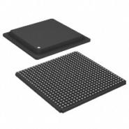
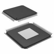
ADSP-2187LBST-160 - Brand New Analog Devices Digital Signal Processors / Controllers (DSPs/DSCs)
-
GENERAL DESCRIPTION
The ADSP-218xL series consists of four single chip microcomputers optimized for digital signal processing applications. The functional block diagram for the ADSP-218xL series members appears in Figure 1 on Page 1. All series members are pin-compatible and are differentiated solely by the amount of on- chip SRAM. This feature, combined with ADSP-21xx code compatibility, provides a great deal of flexibility in the design decision. Specific family members are shown in Table 1.
PERFORMANCE FEATURES
Up to 19 ns instruction cycle time, 52 MIPS sustained performance
Single-cycle instruction execution
Single-cycle context switch
3-bus architecture allows dual operand fetches in every instruction cycle
Multifunction instructions
Power-down mode featuring low CMOS standby power dissipation with 400 CLKIN cycle recovery from power-down condition
Low power dissipation in idle modeINTEGRATION FEATURES
ADSP-2100 family code compatible (easy to use algebraic syntax), with instruction set extensions
Up to 160K bytes of on-chip RAM, configured Up to 32K words program memory RAM Up to 32K words data memory RAM
Dual-purpose program memory for both instruction and data storage
Independent ALU, multiplier/accumulator, and barrel shifter computational units
2 independent data address generators
Powerful program sequencer provides zero overhead looping conditional instruction execution
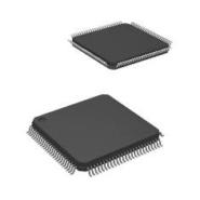
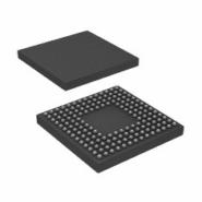
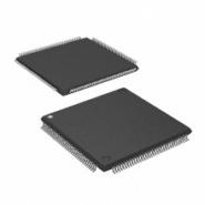
Programmable 16-bit interval timer with prescaler 100-lead LQFP and 144-ball BGASYSTEM INTERFACE FEATURES
16-bit internal DMA port for high-speed access to on-chip memory (mode selectable)
4M-byte memory interface for storage of data tables and program overlays (mode selectable)
8-bit DMA to byte memory for transparent program and data memory transfers (mode selectable)
Programmable memory strobe and separate I/O memory space permits “glueless” system design
Programmable wait state generation
2 double-buffered serial ports with companding hardware and automatic data buffering
Automatic booting of on-chip program memory from bytewide external memory, for example, EPROM, or through internal DMA Port
6 external interrupts
13 programmable flag pins provide flexible system signaling
UART emulation through software SPORT reconfiguration
ICE-Port emulator interface supports debugging in final systems -
Similar parts: 1685 , Click to view
-
Datasheet
-
Shopping guide
Delivery period:
- - Will ship out in 2-3 days
- - DHL Express: 3-7 business days
- - DHL eCommerce: 12-22 business days
- - FedEx International Priority: 3-7 business days
- - EMS: 10-15 business days
Shipping fee:
- - Automatic Email notification (above 5 times)
- - View in your order page
Shipping option:
DHL, FedEx, EMS, SF Express, and Registered Air MailShipping tracking:
- - Automatic Email notification (above 5 times)
- - View in your order page
How to Buy:
- - In-stock, Add to cart > Check out > Submit order > Complete payment >Delivery.
- - Inquiry, Add to inquiry sheet/Submit bom/inquire file/Send email us > Quote > Place order > Complete payment >Delivery.
- View more
Payment:
- - Paypal,Credit Card includes Visa, Master, American Express.
- - Wire transfer, include Local bank transfer.
- - Western Union.
- View more
- Datasheet: Download ADSP-2187LBST-160
- Chipdatas Part: CD92-ADSP-2187LBST-160
- Warehouse: China, Hong Kong
- Dispatch: Within 24 hours
- Free Shipping: Yes
- Prority Shipping: Yes, 3-5 days
- Last Updated: 2024/06/03 08:47 +0800
-
- Full Refund if you don't receive your order
- Full or Partial Refund , If the item is not as described
-
 ADSP-BF533SKBCZ600 - Brand New Analog Devices Digital Signal Processors / Controllers (DSPs/DSCs)160-CSPBGA
 -
 TMS320VC5409GGU100 - Brand New Texas Instruments Digital Signal Processors / Controllers (DSPs/DSCs)144-LFBGA
 -
 TMS320C6211BGFN150 - Brand New Texas Instruments Digital Signal Processors / Controllers (DSPs/DSCs)256-BGA
 -
 TMS320VC5402PGE100 - Brand New Texas Instruments Digital Signal Processors / Controllers (DSPs/DSCs)LQFP-144
 -
 ADSP-BF531SBSTZ400 - Brand New Analog Devices Digital Signal Processors / Controllers (DSPs/DSCs)LQFP-176
 -
 TMS320C6204ZHK200 - Brand New Texas Instruments Digital Signal Processors / Controllers (DSPs/DSCs)288-LFBGA
 -
 DSP56303AG100 - Brand New Freescale / NXP Digital Signal Processors / Controllers (DSPs/DSCs)144-LQFP
 -
 ADSP-TS203SABP-050 - Brand New Analog Devices Digital Signal Processors / Controllers (DSPs/DSCs)576-BBGA Exposed Pad
 -
 ADSP-TS201SABPZ-050 - Brand New Analog Devices Digital Signal Processors / Controllers (DSPs/DSCs)BGA
 -
 ADSP-21489KSWZ-4A - Brand New Analog Devices Digital Signal Processors / Controllers (DSPs/DSCs)100-LQFP Exposed Pad
-
The fee is charged according to the rule of PayPal.
-
The fee is charged according to the rule of PayPal.
-
Western Union charge US$0.00 banking fee.
-
We recommend to use bank transfer for large orders to save on handling fees.
-
DHL(www.dhl.com)
$40 limited time offer. -
UPS(www.ups.com)
$40 limited time offer. -
FedEx(www.fedex.com)
$40 limited time offer. -
Registered Mail(www.singpost.com)
Free shipping without minimum order.
