-
Description
This document provides information on the JS28F256J3D95, which is a Numonyx™ Embedded Flash Memory device. It includes details about its features, operation, and specifications.
Specifications and features
The JS28F256J3D95 has the following specifications and features:
- Architecture:
- Symmetrical 128-Kbyte blocks
- 256 Mbit (256 blocks)
- 128 Mbit (128 blocks)
- 64 Mbit (64 blocks)
- 32 Mbit (32 blocks)
- Performance:
- 75 ns Initial Access Speed (32,64,128 Mbit densities)
- 95 ns Initial Access Speed (256 Mbit only)
- 25 ns 8-word and 4-word Asynchronous page-mode reads
- 32-Byte Write buffer; 4 µs per Byte Effective programming time
- System Voltage:
- VCC = 2.7 V to 3.6 V
- VCCQ = 2.7 V to 3.6 V
- Packaging:
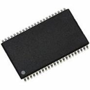
- 56-Lead TSOP (32, 64, 128, 256 Mbit)
- 64-Ball Numonyx Easy BGA package (32, 64, 128 and 256 Mbit)
- Security:
- Enhanced security options for code protection
- 128-bit Protection Register: 64-bits Unique device identifier bits 64-bits User-programmable OTP bits
- Absolute protection with VPEN = GND
- Individual block locking
- Block erase/program lockout during power transitions
- Software:
- Program and erase suspend support
- Flash Data Integrator (FDI), Common Flash Interface (CFI) Compatible
- Quality and Reliability:
- Operating temperature: -40 °C to +85 °C
- 100K Minimum erase cycles per block
- 0.13 µm ETOX™ VIII Process technology
Application Scenarios
The JS28F256J3D95 can be used in various electronic devices that require embedded flash memory. It is suitable for applications that require high performance, security, and reliability.
Comparison
Advantages:
- Symmetrical block architecture allows for efficient organization of data
- Multiple density options available
- Fast initial access speed
- Effective programming time
- Enhanced security options for code protection
- Individual block locking
- Program and erase suspend support
- Compatible with Flash Data Integrator (FDI) and Common Flash Interface (CFI)
- Wide operating temperature range
- High minimum erase cycles per block
- Utilizes advanced ETOX™ VIII Process technology
Disadvantages:
- Higher initial access speed for the 256 Mbit density
- Architecture:
-
Similar parts: 9920 , Click to view
-
Datasheet
-
Shopping guide
Delivery period:
- - Will ship out in 2-3 days
- - DHL Express: 3-7 business days
- - DHL eCommerce: 12-22 business days
- - FedEx International Priority: 3-7 business days
- - EMS: 10-15 business days
Shipping fee:
- - Automatic Email notification (above 5 times)
- - View in your order page
Shipping option:
DHL, FedEx, EMS, SF Express, and Registered Air MailShipping tracking:
- - Automatic Email notification (above 5 times)
- - View in your order page
How to Buy:
- - In-stock, Add to cart > Check out > Submit order > Complete payment >Delivery.
- - Inquiry, Add to inquiry sheet/Submit bom/inquire file/Send email us > Quote > Place order > Complete payment >Delivery.
- View more
Payment:
- - Paypal,Credit Card includes Visa, Master, American Express.
- - Wire transfer, include Local bank transfer.
- - Western Union.
- View more
-
Popular parts of the same kind
Additional Information
- Datasheet: Download JS28F256J3D95
- Chipdatas Part: CD89-JS28F256J3D95
- Warehouse: China, Hong Kong
- Dispatch: Within 24 hours
- Free Shipping: Yes
- Prority Shipping: Yes, 3-5 days
- Last Updated: 2024/06/03 11:24 +0800
Refund
-
- Full Refund if you don't receive your order
- Full or Partial Refund , If the item is not as described
Related Products
-
 M25P80-VMN6TP - Brand New Micron Technology Inc. MemorySOP-8
 -
 MT48LC8M16A2P-6A:L - Brand New Micron Technology Inc. MemoryTSOP-54
 -
 M29W040B-90K1 - Brand New STMicroelectronics MemoryPLCC
 -
 W25Q64BVSFIG - Brand New Winbond Electronics MemorySOP-16
 -
 PC28F128J3D-75 - Brand New INTEI MemoryBGA
 -
 DS1225Y - Brand New Texas Instruments MemoryMOUDLE
 -
 DS2431Q+T&R - Brand New Maxim Integrated Memory6-WDFN Exposed Pad
 -
 IS61LV25616AL-10TLI - Brand New ISSI Memory44-TSOP 0.400", 10.16mm Width
 -
 AT93C66B-XHM-T - Brand New Intel / Altera Memory8-TSSOP 0.173", 4.40mm Width
 -
 AT24C128C-XHM-T - Brand New Intel / Altera MemoryTSSOP
Payment Method
-
The fee is charged according to the rule of PayPal.
-
The fee is charged according to the rule of PayPal.
-
Western Union charge US$0.00 banking fee.
-
We recommend to use bank transfer for large orders to save on handling fees.
Shipping Tips
-
DHL(www.dhl.com)
$40 limited time offer. -
UPS(www.ups.com)
$40 limited time offer. -
FedEx(www.fedex.com)
$40 limited time offer. -
Registered Mail(www.singpost.com)
Free shipping without minimum order.
