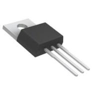
T20N25 - Brand New Alpha & Omega Semiconductor Inc. Field Effect Tube (MOSFET)
-
Description
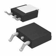
Electronic Component Model T20N25 is a type of Field Effect Tube (MOSFET), particularly designed for low voltage, high speed switching applications in power supplies, converters, and PWM motor controls. It is especially suitable for bridge circuits where diode speed and commutating safe operating areas are critical, with additional safety margins against unexpected voltage transients. The D2PAK package, which houses a larger die than any existing surface mount package, enables it to be used in applications requiring higher power and lower RDS(on) capabilities. This advanced TMOS E-FET is engineered to withstand high energy in the avalanche and commutation modes, and the new energy-efficient design offers a drain-to-source diode with fast recovery time.
Specifications and Features
- Product Category: Field Effect Tube (MOSFET)
- Packaging: D2PAK
- Applications: Power supplies, converters, and PWM motor controls
- Features:
- Avalanche Energy Specified
- Source-to-Drain Diode Recovery Time Comparable to a Discrete Fast Recovery Diode
- Characterized for Use in Bridge Circuits
- IDSS and VDS(on) Specified at Elevated Temperature
- Short Heatsink Tab Manufactured — Not Sheared
- Specially Designed Leadframe for Maximum Power Dissipation
Application Scenarios
The T20N25 electronic component model is ideal for applications requiring low voltage and high-speed switching. It is particularly well-suited for use in bridge circuits, where diode speed and commutating safe operating areas are critical. Its energy-efficient design makes it suitable for a wide range of power supplies, converters, and PWM motor controls.
Comparison
Advantages- Advanced TMOS E-FET technology withstands high energy in the avalanche and commutation modes
- Larger die allows it to be used in applications requiring higher power and lower RDS(on) capabilities
- Energy-efficient design offers a drain-to-source diode with a fast recovery time
- Specially designed leadframe for maximum power dissipation
Disadvantages- The D2PAK package may not be suitable for all surface mount applications
- Pricing may be higher compared to other MOSFET models
-
Similar parts: 25937 , Click to view
-
Datasheet
-
Shopping guide
Delivery period:
- - Will ship out in 2-3 days
- - DHL Express: 3-7 business days
- - DHL eCommerce: 12-22 business days
- - FedEx International Priority: 3-7 business days
- - EMS: 10-15 business days
Shipping fee:
- - Automatic Email notification (above 5 times)
- - View in your order page
Shipping option:
DHL, FedEx, EMS, SF Express, and Registered Air MailShipping tracking:
- - Automatic Email notification (above 5 times)
- - View in your order page
How to Buy:
- - In-stock, Add to cart > Check out > Submit order > Complete payment >Delivery.
- - Inquiry, Add to inquiry sheet/Submit bom/inquire file/Send email us > Quote > Place order > Complete payment >Delivery.
- View more
Payment:
- - Paypal,Credit Card includes Visa, Master, American Express.
- - Wire transfer, include Local bank transfer.
- - Western Union.
- View more
-
Popular parts of the same kind
- Datasheet: Download T20N25
- Chipdatas Part: CD86-T20N25
- Warehouse: China, Hong Kong
- Dispatch: Within 24 hours
- Free Shipping: Yes
- Prority Shipping: Yes, 3-5 days
- Last Updated: 2024/06/03 04:19 +0800
-
- Full Refund if you don't receive your order
- Full or Partial Refund , If the item is not as described
-
 BSP171P H6327 - Brand New Infineon Field Effect Tube (MOSFET)SOT-223
 -
 BSS138PW - Brand New Field Effect Tube (MOSFET)SOT-323
 -
 BSC093N04LSG - Brand New VISHAY Field Effect Tube (MOSFET)TDSON-8
 -
 SI2356DS-T1-GE3 - Brand New VISHAY Field Effect Tube (MOSFET)SOT-23
 -
 2V7002KT1G - Brand New onsemi Field Effect Tube (MOSFET)TO-236-3, SC-59, SOT-23-3
 -
 IRLML2244TRPBF - Brand New IR Field Effect Tube (MOSFET)SOT-23
 -
 IPD50N10S3L-16 - Brand New Intel Field Effect Tube (MOSFET)TO-252-3, DPak 2 Leads + Tab, SC-63
 -
 DMN2075U-7 - Brand New Diodes Incorporated Field Effect Tube (MOSFET)SOT-23
 -
 SI7308DN-T1-GE3 - Brand New ROHM Field Effect Tube (MOSFET)PowerPAK® 1212-8
 -
 2N7002E-T1-E3 - Brand New ROHM Field Effect Tube (MOSFET)TO-236-3, SC-59, SOT-23-3
-
The fee is charged according to the rule of PayPal.
-
The fee is charged according to the rule of PayPal.
-
Western Union charge US$0.00 banking fee.
-
We recommend to use bank transfer for large orders to save on handling fees.
-
DHL(www.dhl.com)
$40 limited time offer. -
UPS(www.ups.com)
$40 limited time offer. -
FedEx(www.fedex.com)
$40 limited time offer. -
Registered Mail(www.singpost.com)
Free shipping without minimum order.
