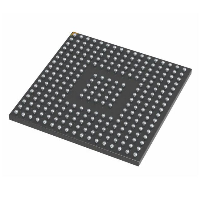
ISPLSI5256VA-125LB272 - Brand New LATTICE Programmable Logic Device (CPLDs/FPGAs)
-
Description
The Electronic Component Model ISPLSI5256VA-125LB272 belongs to the ispLSI 5000V Family of In-System Programmable High Density Logic Devices. It is based on Generic Logic Blocks (GLBs) of 32 registered macrocells and a single Global Routing Pool (GRP) structure for efficient connections across the entire device. The device operates with a 3.3V power supply and supports user-selectable 3.3V/2.5V I/O. It has a capacity of 12000 PLD gates and 256 macrocells. The device also features a high-speed global interconnect, SuperWIDE Input Gating, and interfaces with standard 5V TTL devices. It is available in PCB efficient Ball Grid Array (BGA) package options.
Specifications and features
- 3.3V Power Supply
- User Selectable 3.3V/2.5V I/O
- 12000 PLD Gates / 256 Macrocells
- Up to 192 I/O Pins
- 256 Registers
- High-Speed Global Interconnect
- SuperWIDE 32 Generic Logic Block (GLB) Size for Optimum Performance
- SuperWIDE Input Gating (68 Inputs) for Fast Counters, State Machines, Address Decoders, etc.
- PCB Efficient Ball Grid Array (BGA) Package Options
- Interfaces with Standard 5V TTL Devices
- fmax = 125 MHz Maximum Operating Frequency
- tpd = 7.5 ns Propagation Delay
- Enhanced tsu2 = 7 ns, tsu3 (CLK0/1) = 4.5ns, tsu3 (CLK2/3) = 3.5ns
- TTL/3.3V/2.5V Compatible Input Thresholds and Output Levels
- Electrically Erasable and Reprogrammable
- Non-Volatile
- Programmable Speed/Power Logic Path Optimization
- Increased Manufacturing Yields, Reduced Time-to Market, and Improved Product Quality
- Reprogram Soldered Devices for Faster Debugging
- 100% IEEE 1149.1 BOUNDARY SCAN TESTABLE AND 3.3V IN-SYSTEM PROGRAMMABLE
- Enhanced Pin-Locking Architecture with Single Level Global Routing Pool and SuperWIDE GLBs
- Wrap Around Product Term Sharing Array Supports up to 35 Product Terms Per Macrocell
- Macrocells Support Concurrent Combinatorial and Registered Functions
- Macrocell Registers Feature Multiple Control Options Including Set, Reset and Clock Enable
- Four Dedicated Clock Input Pins Plus Macrocell Product Term Clocks
- Slew and Skew Programmable I/O (SASPI/O™) Supports Programmable Bus Hold, Pull-up, Open Drain and Slew and Skew Rate Options
- Six Global Output Enable Terms, Two Global OE Pins and One Product Term OE per Macrocell
- ispDesignEXPERT™ - Logic Compiler and Complete isp Device Design Systems from HDL Synthesis through In-System Programming
- Superior Quality of Results
- Tightly Integrated with Leading CAE Vendor Tools
- Productivity Enhancing Timing Analyzer, Explore Tools, Timing Simulator and ispANALYZER™
- PC and UNIX Platforms
Application Scenarios
The ISPLSI5256VA-125LB272 can be used in various applications including fast counters, state machines, address decoders, and more. Its SuperWIDE Input Gating and high-speed global interconnect make it ideal for designs that require optimum performance. The device is also compatible with standard 5V TTL devices, making it versatile and widely applicable.
Comparison
Advantages- High density with 12000 PLD Gates / 256 Macrocells
- User-selectable 3.3V/2.5V I/O
- SuperWIDE Input Gating for fast counters, state machines, address decoders, etc.
- High-speed global interconnect
- Interfaces with standard 5V TTL devices
- Programmable Speed/Power Logic Path Optimization
- In-system programmable for increased manufacturing yields and reduced time-to-market
- Supports IEEE 1149.1 boundary scan testing
- Architecture features such as enhanced pin-locking and wrap around product term sharing array
- Integrated logic compiler and design systems for seamless development
Disadvantages- Limited maximum operating frequency of 125 MHz
- Proprietary BGA package options
-
Similar parts: 2518 , Click to view
-
Datasheet
-
Shopping guide
Delivery period:
- - Will ship out in 2-3 days
- - DHL Express: 3-7 business days
- - DHL eCommerce: 12-22 business days
- - FedEx International Priority: 3-7 business days
- - EMS: 10-15 business days
Shipping fee:
- - Automatic Email notification (above 5 times)
- - View in your order page
Shipping option:
DHL, FedEx, EMS, SF Express, and Registered Air MailShipping tracking:
- - Automatic Email notification (above 5 times)
- - View in your order page
How to Buy:
- - In-stock, Add to cart > Check out > Submit order > Complete payment >Delivery.
- - Inquiry, Add to inquiry sheet/Submit bom/inquire file/Send email us > Quote > Place order > Complete payment >Delivery.
- View more
Payment:
- - Paypal,Credit Card includes Visa, Master, American Express.
- - Wire transfer, include Local bank transfer.
- - Western Union.
- View more
- Datasheet: Download ISPLSI5256VA-125LB272
- Chipdatas Part: CD93-ISPLSI5256VA-125LB272
- Warehouse: China, Hong Kong
- Dispatch: Within 24 hours
- Free Shipping: Yes
- Prority Shipping: Yes, 3-5 days
- Last Updated: 2024/09/21 08:44 +0800
-
- Full Refund if you don't receive your order
- Full or Partial Refund , If the item is not as described
-
 LCMXO2-640HC-4TG100C - Brand New LATTICE Programmable Logic Device (CPLDs/FPGAs)QFP-100
 -
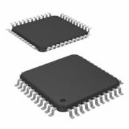
 LC4032V-75TN48C - Brand New Lattice Semiconductor Programmable Logic Device (CPLDs/FPGAs)48-LQFP
 -
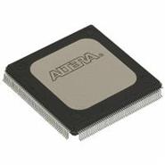
 EPM3128ATC144-10N - Brand New Intel / Altera Programmable Logic Device (CPLDs/FPGAs)QFP
 -
 XC9572-7PC44C - Brand New XILINX Programmable Logic Device (CPLDs/FPGAs)44-LCC J-Lead
 -
 M4A3-32/32-10VC - Brand New Lattice Semiconductor Programmable Logic Device (CPLDs/FPGAs)44-TQFP
 -
 EPM3032ATC44-10N - Brand New Intel / Altera Programmable Logic Device (CPLDs/FPGAs)QFP-44
 -
LCMXO1200C-3FTN256C - Brand New Lattice Semiconductor Programmable Logic Device (CPLDs/FPGAs)256-LBGA
-
 EPM7256SRI208-10N - Brand New Intel / Altera Programmable Logic Device (CPLDs/FPGAs)QFP
 -
 XC9572XL-10TQ100I - Brand New XILINX Programmable Logic Device (CPLDs/FPGAs)TQFP
 -
 EPM1270T144I5N - Brand New Intel / Altera Programmable Logic Device (CPLDs/FPGAs)144-LQFP
-
The fee is charged according to the rule of PayPal.
-
The fee is charged according to the rule of PayPal.
-
Western Union charge US$0.00 banking fee.
-
We recommend to use bank transfer for large orders to save on handling fees.
-
DHL(www.dhl.com)
$40 limited time offer. -
UPS(www.ups.com)
$40 limited time offer. -
FedEx(www.fedex.com)
$40 limited time offer. -
Registered Mail(www.singpost.com)
Free shipping without minimum order.
