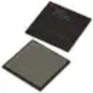
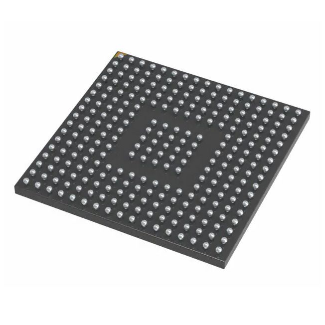
XCF32PFSG48C - Brand New XILINX Memory - Configuration Proms for FPGAs
-
Description
The XCF32PFSG48C model is an electronic component belonging to the memory configuration PROMs for FPGAs product category. It boasts a wide range of features such as a voltage range of 1.71 to 3.6V for operating and flash write, a temperature range of -40 to 105°C, and a clock system that includes a 3 to 32 MHz crystal oscillator, 32 kHz crystal oscillator, and a multi-purpose clock generator. Additionally, it has a 10 low-power mode system with a memory protection unit, multi-master protection, and other peripheral functions.
Specifications and features
The XCF32PFSG48C model features:
- Operating Characteristics: Voltage range of 1.71 to 3.6V, flash write voltage range of 1.71 to 3.6V, and a temperature range of -40 to 105°C.
- Performance: Up to 100 MHz ARM Cortex-M4 core with DSP instructions delivering 1.25 Dhrystone MIPS per MHz.
- Memories and memory interfaces: Up to 512 KB program flash memory on non FlexMemory devices, up to 128 KB RAM, serial programming interface (EzPort), and FlexBus external bus interface.
- Clocks: 3 to 32 MHz crystal oscillator, 32 kHz crystal oscillator, and a multi-purpose clock generator.
- System peripherals: 10 low-power modes to provide power optimization based on application requirements, memory protection unit with multi-master protection, 16-channel DMA controller, supporting up to 64 request sources, external watchdog monitor, software watchdog, and low-leakage wakeup unit.
- Security and integrity modules: Hardware CRC module to support fast cyclic redundancy checks, and a 128-bit unique identification (ID) number per chip.
- Human-machine interface: Low-power hardware touch sensor interface (TSI), and general-purpose input/output.
- Analog modules: Two 16-bit SAR ADCs, programmable gain amplifier (up to x64) integrated into each ADC, 12-bit DAC, three analog comparators (CMP) containing a 6-bit DAC and programmable reference input, and voltage reference.
- Timers: Programmable delay block, eight-channel motor control/general purpose/PWM timer, two 2-channel quadrature decoder/general purpose timers, periodic interrupt timers, 16-bit low-power timer, carrier modulator transmitter, and real-time clock.
- Communication interfaces: USB full-/low-speed On-the-Go controller with on chip transceiver, two Controller Area Network (CAN) modules, three SPI modules, two I2C modules, five UART modules, Secure Digital host controller (SDHC), and I2S module.
Application Scenarios
The XCF32PFSG48C model is commonly used for applications requiring memory configuration PROMs for FPGAs. It can be used in various human-machine interface scenarios, as well as in communication interfaces for data transfer. It can also be used in analog modules for voltage reference and SAR ADCs.
Comparison
Advantages- Wide range of operating voltage (1.71 to 3.6V) and flash write voltage range (1.71 to 3.6V).
- A multi-purpose clock generator and 32 kHz crystal oscillator are included.
- Features a hardware CRC module to support fast cyclic redundancy checks and a 128-bit unique identification (ID) number per chip for security and integrity modules.
- Provides up to 512 KB program flash memory on non FlexMemory devices and up to 128 KB RAM for memories and memory interfaces.
- Includes a USB full-/low-speed On-the-Go controller with on chip transceiver for communication interfaces.
Disadvantages- May not be compatible with all FPGAs.
- Temperature range (ambient) is limited to -40 to 105°C.
- Some of the features may not be applicable to certain applications.
-
Similar parts: 289 , Click to view
-
Datasheet
-
Shopping guide
Delivery period:
- - Will ship out in 2-3 days
- - DHL Express: 3-7 business days
- - DHL eCommerce: 12-22 business days
- - FedEx International Priority: 3-7 business days
- - EMS: 10-15 business days
Shipping fee:
- - Automatic Email notification (above 5 times)
- - View in your order page
Shipping option:
DHL, FedEx, EMS, SF Express, and Registered Air MailShipping tracking:
- - Automatic Email notification (above 5 times)
- - View in your order page
How to Buy:
- - In-stock, Add to cart > Check out > Submit order > Complete payment >Delivery.
- - Inquiry, Add to inquiry sheet/Submit bom/inquire file/Send email us > Quote > Place order > Complete payment >Delivery.
- View more
Payment:
- - Paypal,Credit Card includes Visa, Master, American Express.
- - Wire transfer, include Local bank transfer.
- - Western Union.
- View more
-
Popular parts of the same kind
- Datasheet: Download XCF32PFSG48C
- Chipdatas Part: CD91-XCF32PFSG48C
- Warehouse: China, Hong Kong
- Dispatch: Within 24 hours
- Free Shipping: Yes
- Prority Shipping: Yes, 3-5 days
- Last Updated: 2024/06/03 06:23 +0800
-
- Full Refund if you don't receive your order
- Full or Partial Refund , If the item is not as described
-
 XCF08PVOG48C - Brand New XILINX Memory - Configuration Proms for FPGAsTSOP-48
 -
 XC18V04VQG44C - Brand New XILINX Memory - Configuration Proms for FPGAs44-TQFP
 -
 EPCQ256SI16N - Brand New Intel / Altera Memory - Configuration Proms for FPGAsSOP-16
 -
XCF32PFSG48C - Brand New XILINX Memory - Configuration Proms for FPGAsBGA
-
 XCF128XFTG64C - Brand New XILINX Memory - Configuration Proms for FPGAsFTBGA-64
 -
 XCF02SVOG20C - Brand New XILINX Memory - Configuration Proms for FPGAsSOP
 -
 EPCS64SI16N - Brand New Intel / Altera Memory - Configuration Proms for FPGAsSOIC-16
 -
 XCF16PFS48C - Brand New XILINX Memory - Configuration Proms for FPGAsBGA
 -
 EPC1PI8N - Brand New Intel / Altera Memory - Configuration Proms for FPGAsDIP-8
 -
 XC18V04VQG44C - Brand New XILINX Memory - Configuration Proms for FPGAsQFP-4410x10
-
The fee is charged according to the rule of PayPal.
-
The fee is charged according to the rule of PayPal.
-
Western Union charge US$0.00 banking fee.
-
We recommend to use bank transfer for large orders to save on handling fees.
-
DHL(www.dhl.com)
$40 limited time offer. -
UPS(www.ups.com)
$40 limited time offer. -
FedEx(www.fedex.com)
$40 limited time offer. -
Registered Mail(www.singpost.com)
Free shipping without minimum order.
