-
56F8033/56F8023 Description
The 56F8033/56F8023 is a member of the 56800E core-based family of Digital Signal Controllers (DSCs). It combines, on a single chip, the processing power of a DSP and the functionality of a microcontroller with a flexible set of peripherals to create an extremely cost-effective solution. Because of its low cost, configuration flexibility, and compact program code, the 56F8033/56F8023 is well-suited for many applications. The 56F8033/56F8023 includes many peripherals that are especially useful for industrial control, motion control, home appliances, general-purpose inverters, smart sensors, fire and security systems, switched-mode power supply, power management, and medical monitoring applications.
The 56800E core is based on a dual Harvard-style architecture consisting of three execution units operating in parallel, allowing as many as six operations per instruction cycle. The MCU-style programming model and optimized instruction set allow straightforward generation of efficient, compact DSP and control code. The instruction set is also highly efficient for C compilers to enable rapid development of optimized control applications.56F8033/56F8023 General Description
• Up to 32 MIPS at 32MHz core frequency
• DSP and MCU functionality in a unified, C-efficient architecture
• 56F8033 offers 64KB (32K x 16) Program Flash
• 56F8023 offers 32KB (16K x 16) Program Flash
• 56F8033 offers 8KB (4K x 16) Unified Data/Program RAM
• 56F8023 offers 4KB (2K x 16) Unified Data/Program RAM
• One 6-channel PWM module
• Two 3-channel 12-bit Analog-to-Digital Converters (ADCs)
• Two Internal 12-bit Digital-to-Analog Converters (DACs)
• Two Analog Comparators
• One Programmable Interval Timer (PIT)
• One Queued Serial Communication Interface (QSCI) with LIN slave functionality
• One Queued Serial Peripheral Interfaces (QSPI)
• One 16-bit Quad Timer
• One Inter-Integrated Circuit (I2C) port
• Computer Operating Properly (COP)/Watchdog
• On-Chip Relaxation Oscillator
• Integrated Power-On Reset (POR) and Low-Voltage Interrupt (LVI) Module
• JTAG/Enhanced On-Chip Emulation (OnCE™) for unobtrusive, real-time debugging
• Up to 26 GPIO lines
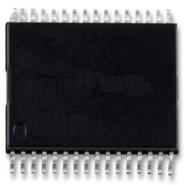
• 32-pin LQFP Package56F8033/56F8023 Features
Digital Signal Controller Core
• Efficient 16-bit 56800E family Digital Signal Controller (DSC) engine with dual Harvard architecture
• As many as 32 Million Instructions Per Second (MIPS) at 32MHz core frequency
• Single-cycle 16 × 16-bit parallel Multiplier-Accumulator (MAC)
• Four 36-bit accumulators, including extension bits
• 32-bit arithmetic and logic multi-bit shifter
• Parallel instruction set with unique DSP addressing modes
• Hardware DO and REP loops
• Three internal address buses
• Four internal data buses
• Instruction set supports both DSP and controller functions
• Controller-style addressing modes and instructions for compact code
• Efficient C compiler and local variable support
• Software subroutine and interrupt stack with depth limited only by memory
• JTAG/Enhanced On-Chip Emulation (OnCE) for unobtrusive, processor speed- independent, real-time debuggingMemory
• Dual Harvard architecture permits as many as three simultaneous accesses to program and data memory
• Flash security and protection that prevent unauthorized users from gaining access to the internal Flash
• On-chip memory— Master and slave modes
— Four-words-deep FIFOs available on both transmitter and receiver
— Programmable Length Transactions (2 to 16 bits)
• One Inter-Integrated Circuit (I2C) port
— Operates up to 400kbps
— Supports both master and slave operation
— Supports both 10-bit address mode and broadcasting mode
• One 16-bit Programmable Interval Timer (PIT)
• Two analog Comparators (CMPs)
— Selectable input source includes external pins, DACs
— Programmable output polarity
— Output can drive Timer input, PWM fault input, PWM source, external pin output and trigger ADCs
— Output falling and rising edge detection able to generate interrupts
• Computer Operating Properly (COP)/Watchdog timer capable of selecting different clock sources
• Up to 26 General-Purpose I/O (GPIO) pins with 5V tolerance
• Integrated Power-On Reset and Low-Voltage Interrupt Module
• Phase Lock Loop (PLL) provides a high-speed clock to the core and peripherals
• Clock sources:
— On-chip relaxation oscillator
— External clock: Crystal oscillator, ceramic resonator, and external clock source
• JTAG/EOnCE debug programming interface for real-time debugging
1.1.5 Energy Information
• Fabricated in high-density CMOS with 5V tolerance
• On-chip regulators for digital and analog circuitry to lower cost and reduce noise
• Wait and Stop modes available
• ADC smart power management
• Each peripheral can be individually disabled to save power— 64KB of Program Flash (56F80233 device)
32KB of Program Flash (56F8023 device)
— 8KB of Unified Data/Program RAM (56F8033 device)
4KB of Unified Data/Program RAM (56F8023 device)
• EEPROM emulation capability using FlashPeripheral Circuits for 56F8033/56F8023
• One multi-function six-output Pulse Width Modulator (PWM) module
— Up to 96MHz PWM operating clock
— 15 bits of resolution
— Center-aligned and edge-aligned PWM signal mode
— Four programmable fault inputs with programmable digital filter
— Double-buffered PWM registers
— Each complementary PWM signal pair allows selection of a PWM supply source from:
– PWM generator
– External GPIO
– Internal timers
– Analog comparator outputs
– ADC conversion result which compares with values of ADC high- and low-limit registers to set PWM output
• Two independent 12-bit Analog-to-Digital Converters (ADCs)
— 2 x 3 channel inputs
— Supports both simultaneous and sequential conversions
— ADC conversions can be synchronized by both PWM and timer modules
— Sampling rate up to 2.67MSPS
— 16-word result buffer registers
• Two internal 12-bit Digital-to-Analog Converters (DACs)
— 2 μs settling time when output swing from rail to rail
— Automatic waveform generation generates square, triangle and sawtooth waveforms with programmable period, update rate, and range
• One 16-bit multi-purpose Quad Timer module (TMR)
— Up to 96MHz operating clock
— Eight independent 16-bit counter/timers with cascading capability
— Each timer has capture and compare capability
— Up to 12 operating modes
• One Queued Serial Communication Interface (QSCI) with LIN Slave functionality
— Full-duplex or single-wire operation
— Two receiver wake-up methods:
– Idle line
– Address mark
— Four-bytes-deep FIFOs are available on both transmitter and receiver
• One Queued Serial Peripheral Interfaces (QSPI)
— Full-duplex operation
— Master and slave modes
— Four-words-deep FIFOs available on both transmitter and receiver
— Programmable Length Transactions (2 to 16 bits)
• One Inter-Integrated Circuit (I2C) port
— Operates up to 400kbps
— Supports both master and slave operation
— Supports both 10-bit address mode and broadcasting mode
• One 16-bit Programmable Interval Timer (PIT)
• Two analog Comparators (CMPs)
— Selectable input source includes external pins, DACs
— Programmable output polarity
— Output can drive Timer input, PWM fault input, PWM source, external pin output and trigger ADCs
— Output falling and rising edge detection able to generate interrupts
• Computer Operating Properly (COP)/Watchdog timer capable of selecting different clock sources
• Up to 26 General-Purpose I/O (GPIO) pins with 5V tolerance
• Integrated Power-On Reset and Low-Voltage Interrupt Module
• Phase Lock Loop (PLL) provides a high-speed clock to the core and peripherals
• Clock sources:
— On-chip relaxation oscillator
— External clock: Crystal oscillator, ceramic resonator, and external clock source
• JTAG/EOnCE debug programming interface for real-time debuggingEnergy Information
• Fabricated in high-density CMOS with 5V tolerance
• On-chip regulators for digital and analog circuitry to lower cost and reduce noise
• Wait and Stop modes available
• ADC smart power management
• Each peripheral can be individually disabled to save power -
Similar parts: 430483 , Click to view
-
Datasheet
-
Shopping guide
Delivery period:
- - Will ship out in 2-3 days
- - DHL Express: 3-7 business days
- - DHL eCommerce: 12-22 business days
- - FedEx International Priority: 3-7 business days
- - EMS: 10-15 business days
Shipping fee:
- - Automatic Email notification (above 5 times)
- - View in your order page
Shipping option:
DHL, FedEx, EMS, SF Express, and Registered Air MailShipping tracking:
- - Automatic Email notification (above 5 times)
- - View in your order page
How to Buy:
- - In-stock, Add to cart > Check out > Submit order > Complete payment >Delivery.
- - Inquiry, Add to inquiry sheet/Submit bom/inquire file/Send email us > Quote > Place order > Complete payment >Delivery.
- View more
Payment:
- - Paypal,Credit Card includes Visa, Master, American Express.
- - Wire transfer, include Local bank transfer.
- - Western Union.
- View more
-
Popular parts of the same kind
- Datasheet: Download F8033J
- Chipdatas Part: CD90-F8033J
- Warehouse: China, Hong Kong
- Dispatch: Within 24 hours
- Free Shipping: Yes
- Prority Shipping: Yes, 3-5 days
- Last Updated: 2024/09/28 21:24 +0800
-
- Full Refund if you don't receive your order
- Full or Partial Refund , If the item is not as described
-
The fee is charged according to the rule of PayPal.
-
The fee is charged according to the rule of PayPal.
-
Western Union charge US$0.00 banking fee.
-
We recommend to use bank transfer for large orders to save on handling fees.
-
DHL(www.dhl.com)
$40 limited time offer. -
UPS(www.ups.com)
$40 limited time offer. -
FedEx(www.fedex.com)
$40 limited time offer. -
Registered Mail(www.singpost.com)
Free shipping without minimum order.

