S25FL032P0XMFI010 - Brand New Cypress Semiconductor Memory
-
General Description
The S25FL032P is a 3.0 V (2.7 V to 3.6 V), single-power-supply Flash memory device. The device consists of 64 uniform 64-KB sectors with the two (top or bottom) 64-KB sectors further split up into thirty-two 4-KB sub sectors. The S25FL032P device is fully backward compatible with the S25FL032A device.
The device accepts data written to Serial Input (SI) and outputs data on Serial Output (SO). The devices are designed to be programmed in-system with the standard system 3.0-V VCC supply.**The S25FL032P device adds the following high-performance features using
five new instructions:**
■ Dual Output Read using both SI and SO pins as output pins at a clock rate of up to 80 MHz
■ Quad Output Read using SI, SO, W#/ACC, and HOLD# pins as output pins at a clock
rate of up to 80 MHz
■ Dual I/O High Performance Read using both SI and SO pins as input and output pins at a clock
rate of up to 80 MHz
■ Quad I/O High Performance Read using SI, SO, W#/ACC, and HOLD# pins as input and output
pins at a clock rate of up to 80 MHz
■ Quad Page Programming using SI, SO, W#/ACC, and HOLD# pins as input pins to program data
at a clock rate of up to 80 MHzDistinctive Characteristics
Architectural Advantages
■ Single power supply operation
– Full voltage range: 2.7 V to 3.6 V read and write operations
■ Memory architecture
– Uniform 64-KB sectors
– Top or bottom parameter block (two 64-KB sectors (top
or bottom) broken down into 16 4-KB sub-sectors each)
– 256-byte page size
– Backward compatible with the S25FL032A device
■ Program
– Page Program (up to 256 bytes) in 1.5 ms (typical)
– Program operations are on a page by page basis
– Accelerated programming mode via 9-V W#/ACC pin
– Quad Page Programming
■ Erase
– Bulk erase function
– Sector erase (SE) command (D8h) for 64-KB sectors
– Sub-sector erase (P4E) command (20h) for 4-KB sectors
– Sub-sector erase (P8E) command (40h) for 8-KB sectors
■ Cycling endurance
– 100,000 cycles per sector typical
■ Data retention
– 20 years typical
■ Device ID
– JEDEC standard two-byte electronic signature
– RES command one-byte electronic signature for backward
compatibility
■ One time programmable (OTP) area for permanent, secure
identification; can be programmed and locked at the factory
or by the customer
■ Common Flash Interface (CFI) compliant: allows host system
to identify and accommodate multiple flash devices
■ Process technology
– Manufactured on 0.09 μm MirrorBit® process technology
■ Package option
– Industry Standard Pinouts
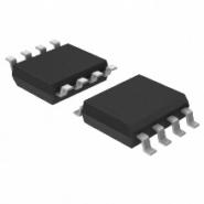
– 8-pin SO package (208 mils)
– 16-pin SO package (300 mils)
– 8-contact USON package (5 x 6 mm)
– 8-contact WSON package (6 x 8 mm)
– 24-ball BGA 6 x 8 mm package, 5 x 5 pin configuration
– 24-ball BGA 6 x 8 mm package, 6 x 4 pin configurationPerformance Characteristics
■ Speed
– Normal READ (Serial): 40-MHz clock rate
– FAST_READ (Serial): 104-MHz clock rate (maximum)
– DUAL I/O FAST_READ: 80-MHz clock rate or
20 MB/s effective data rate
– QUAD I/O FAST_READ: 80 MHz clock rate or
40 MB/s effective data rate
■ Power saving standby mode
– Standby Mode 80 μA (typical)
– Deep Power-Down Mode 3 μA (typical)
Memory Protection Features
■ Memory protection
– W#/ACC pin works in conjunction with Status Register Bits
to protect specified memory areas
– Status Register Block Protection bits (BP2, BP1, BP0) in
status register configure parts of memory as read-only -
Similar parts: 9920 , Click to view
-
Datasheet
-
Shopping guide
Delivery period:
- - Will ship out in 2-3 days
- - DHL Express: 3-7 business days
- - DHL eCommerce: 12-22 business days
- - FedEx International Priority: 3-7 business days
- - EMS: 10-15 business days
Shipping fee:
- - Automatic Email notification (above 5 times)
- - View in your order page
Shipping option:
DHL, FedEx, EMS, SF Express, and Registered Air MailShipping tracking:
- - Automatic Email notification (above 5 times)
- - View in your order page
How to Buy:
- - In-stock, Add to cart > Check out > Submit order > Complete payment >Delivery.
- - Inquiry, Add to inquiry sheet/Submit bom/inquire file/Send email us > Quote > Place order > Complete payment >Delivery.
- View more
Payment:
- - Paypal,Credit Card includes Visa, Master, American Express.
- - Wire transfer, include Local bank transfer.
- - Western Union.
- View more
-
Popular parts of the same kind
- Datasheet: Download S25FL032P0XMFI010
- Chipdatas Part: CD93-S25FL032P0XMFI010
- Warehouse: China, Hong Kong
- Dispatch: Within 24 hours
- Free Shipping: Yes
- Prority Shipping: Yes, 3-5 days
- Last Updated: 2024/09/28 21:21 +0800
-
- Full Refund if you don't receive your order
- Full or Partial Refund , If the item is not as described
-
 M25P80-VMN6TP - Brand New Micron Technology Inc. MemorySOP-8
 -
 MT48LC8M16A2P-6A:L - Brand New Micron Technology Inc. MemoryTSOP-54
 -
 M29W040B-90K1 - Brand New STMicroelectronics MemoryPLCC
 -
 W25Q64BVSFIG - Brand New Winbond Electronics MemorySOP-16
 -
 PC28F128J3D-75 - Brand New INTEI MemoryBGA
 -
 DS1225Y - Brand New Texas Instruments MemoryMOUDLE
 -
 DS2431Q+T&R - Brand New Maxim Integrated Memory6-WDFN Exposed Pad
 -
 IS61LV25616AL-10TLI - Brand New ISSI Memory44-TSOP 0.400", 10.16mm Width
 -
 AT93C66B-XHM-T - Brand New Intel / Altera Memory8-TSSOP 0.173", 4.40mm Width
 -
 AT24C128C-XHM-T - Brand New Intel / Altera MemoryTSSOP
-
The fee is charged according to the rule of PayPal.
-
The fee is charged according to the rule of PayPal.
-
Western Union charge US$0.00 banking fee.
-
We recommend to use bank transfer for large orders to save on handling fees.
-
DHL(www.dhl.com)
$40 limited time offer. -
UPS(www.ups.com)
$40 limited time offer. -
FedEx(www.fedex.com)
$40 limited time offer. -
Registered Mail(www.singpost.com)
Free shipping without minimum order.
