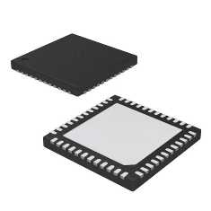
LCMXO2-1200UHC-4FTG256I - Brand New Lattice Semiconductor Programmable Logic Device (CPLDs/FPGAs)
-
Description
Electronic Component Model: LCMXO2-1200UHC-4FTG256I is a programmable logic device (CPLD/FPGA). It offers a flexible logic architecture with six devices ranging from 256 to 6864 LUT4s and 19 to 335 I/Os. This component is designed with an advanced 65 nm low-power process, resulting in ultra-low power consumption, as low as 19 µW in standby mode. It also features embedded and distributed memory, including up to 240 Kbits sysMEM™ Embedded Block RAM and up to 54 Kbits Distributed RAM. Furthermore, it has a dedicated FIFO control logic and on-chip user flash memory with up to 256 Kbits of memory capacity. The user flash memory can be accessed through various interfaces like WISHBONE, SPI, I2C, and JTAG. Additionally, this component supports pre-engineered source synchronous I/O with DDR registers in I/O cells, dedicated gearing logic, and various DDR memory options. It also offers a high-performance, flexible I/O buffer that supports a wide range of interfaces, including LVCMOS, LVTTL, PCI, LVDS, Bus-LVDS, MLVDS, RSDS, LVPECL, SSTL, HSTL, and Schmitt trigger inputs with up to 0.5V hysteresis. The I/Os support hot socketing and have on-chip differential termination with programmable pull-up or pull-down modes.
Specifications and features
Flexible Logic Architecture
- Six devices with 256 to 6864 LUT4s and 19 to 335 I/Os
Ultra Low Power Devices
- Advanced 65 nm low power process
- As low as 19 µW standby power
- Programmable low swing differential I/Os
- Stand-by mode and other power saving options
Embedded and Distributed Memory
- Up to 240 Kbits sysMEM™ Embedded Block RAM
- Up to 54 Kbits Distributed RAM
- Dedicated FIFO control logic On-Chip User Flash Memory
- Up to 256 Kbits of User Flash Memory
- 100,000 write cycles
- Accessible through WISHBONE, SPI, I2C, and JTAG interfaces
- Can be used as soft processor PROM or as Flash memory
Pre-Engineered Source Synchronous I/O
- DDR registers in I/O cells
- Dedicated gearing logic
- 7:1 Gearing for Display I/Os
- Generic DDR, DDRX2, DDRX4
- Dedicated DDR/DDR2/LPDDR memory with DQS support
High Performance, Flexible I/O Buffer
- Programmable sysIO™ buffer supports wide range of interfaces:
- LVCMOS 3.3/2.5/1.8/1.5/1.2
- LVTTL
- PCI
- LVDS, Bus-LVDS, MLVDS, RSDS, LVPECL
- SSTL 25/18
- HSTL 18
- Schmitt trigger inputs, up to 0.5V hysteresis
- I/Os support hot socketing
- On-chip differential termination
- Programmable pull-up or pull-down mode
Application Scenarios
This electronic component is ideal for applications that require programmable logic, such as digital signal processing, telecommunications, industrial control systems, and consumer electronics. Its flexible logic architecture, low power consumption, and various memory options make it suitable for a wide range of applications. Additionally, its support for different interfaces and I/O buffer features enhance its versatility.
Comparison
Advantages- Flexible logic architecture with a wide range of LUT4s and I/Os
- Ultra-low power consumption with advanced 65nm low-power process
- Diverse memory options, including embedded block RAM and user flash memory
- Supports various interfaces and I/O buffer features
- Can be used for different applications, including digital signal processing and telecommunications
Disadvantages- May have a learning curve for beginners due to the complexity of the programmable logic
- Requires an understanding of FPGA design principles
-
Similar parts: 2518 , Click to view
-
Datasheet
-
Shopping guide
Delivery period:
- - Will ship out in 2-3 days
- - DHL Express: 3-7 business days
- - DHL eCommerce: 12-22 business days
- - FedEx International Priority: 3-7 business days
- - EMS: 10-15 business days
Shipping fee:
- - Automatic Email notification (above 5 times)
- - View in your order page
Shipping option:
DHL, FedEx, EMS, SF Express, and Registered Air MailShipping tracking:
- - Automatic Email notification (above 5 times)
- - View in your order page
How to Buy:
- - In-stock, Add to cart > Check out > Submit order > Complete payment >Delivery.
- - Inquiry, Add to inquiry sheet/Submit bom/inquire file/Send email us > Quote > Place order > Complete payment >Delivery.
- View more
Payment:
- - Paypal,Credit Card includes Visa, Master, American Express.
- - Wire transfer, include Local bank transfer.
- - Western Union.
- View more
- Datasheet: Download LCMXO2-1200UHC-4FTG256I
- Chipdatas Part: CD93-LCMXO2-1200UHC-4FTG256I
- Warehouse: China, Hong Kong
- Dispatch: Within 24 hours
- Free Shipping: Yes
- Prority Shipping: Yes, 3-5 days
- Last Updated: 2024/06/03 07:56 +0800
-
- Full Refund if you don't receive your order
- Full or Partial Refund , If the item is not as described
-
 LCMXO2-640HC-4TG100C - Brand New LATTICE Programmable Logic Device (CPLDs/FPGAs)QFP-100
 -
 LC4032V-75TN48C - Brand New Lattice Semiconductor Programmable Logic Device (CPLDs/FPGAs)48-LQFP
 -
 EPM3128ATC144-10N - Brand New Intel / Altera Programmable Logic Device (CPLDs/FPGAs)QFP
 -
 XC9572-7PC44C - Brand New XILINX Programmable Logic Device (CPLDs/FPGAs)44-LCC J-Lead
 -
 M4A3-32/32-10VC - Brand New Lattice Semiconductor Programmable Logic Device (CPLDs/FPGAs)44-TQFP
 -
 EPM3032ATC44-10N - Brand New Intel / Altera Programmable Logic Device (CPLDs/FPGAs)QFP-44
 -
LCMXO1200C-3FTN256C - Brand New Lattice Semiconductor Programmable Logic Device (CPLDs/FPGAs)256-LBGA
-
 EPM7256SRI208-10N - Brand New Intel / Altera Programmable Logic Device (CPLDs/FPGAs)QFP
 -
 XC9572XL-10TQ100I - Brand New XILINX Programmable Logic Device (CPLDs/FPGAs)TQFP
 -
 EPM1270T144I5N - Brand New Intel / Altera Programmable Logic Device (CPLDs/FPGAs)144-LQFP
-
The fee is charged according to the rule of PayPal.
-
The fee is charged according to the rule of PayPal.
-
Western Union charge US$0.00 banking fee.
-
We recommend to use bank transfer for large orders to save on handling fees.
-
DHL(www.dhl.com)
$40 limited time offer. -
UPS(www.ups.com)
$40 limited time offer. -
FedEx(www.fedex.com)
$40 limited time offer. -
Registered Mail(www.singpost.com)
Free shipping without minimum order.
