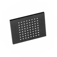
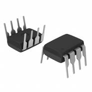
AT17F040A-30QC - Brand New Intel / Altera Memory - Configuration Proms for FPGAs
-
Description
The AT17F040A-30QC is an FPGA Configuration EEPROM (Configurator) that provides an easy-to-use, cost-effective configuration memory for Field Programmable Gate Arrays. It is part of the AT17 Series and is available in the 8-pin DIP and the popular 20-pin PLCC and SOIC packages. The AT17F040A-30QC uses a simple serial-access procedure to configure one or more FPGA devices. It offers enough memory to configure one or multiple smaller FPGAs. Additionally, it has the ability to select the polarity of the reset function through EEPROM programming. The AT17F040A-30QC can be programmed with industry standard programmers.
Specifications and features
- E2 Programmable 65,536 x 1, 131,072 x 1, and 262,144 x 1 bit Serial Memories Designed to Store Configuration Programs For Programmable Gate Arrays
- Simple Interface to SRAM FPGAs Requires Only One User I/O Pin
- Compatible With AT6000 FPGAs, ATT3000 FPGA, EPF8000 FPGAs, ORCA FPGAs, XC2000, XC3000, XC4000, XC5000 FPGAs, MPA1000
- Cascadable To Support Additional Configurations or Future Higher-density Arrays (17C128 and 17C256 only)
- Low-power CMOS EEPROM Process
- Programmable Reset Polarity
- Available In the Space-efficient Plastic DIP or Surface-mount PLCC and SOIC Packages
- In-System Programmable Via 2-Wire Bus
- Emulation of 24CXX Serial EPROMs
- Available in 3.3V ± 10% LV Version
Application Scenarios
The AT17F040A-30QC is designed for use in configuring Field Programmable Gate Arrays. It is compatible with a wide range of FPGAs, making it suitable for various applications in industries such as telecommunications, automotive, aerospace, and more. It can be used to store configuration programs for programmable gate arrays and offers a simple interface to SRAM FPGAs.
Comparison
Advantages:
- Easy-to-use and cost-effective configuration memory
- Simple serial-access procedure for configuring FPGAs
- Ability to select reset polarity through EEPROM programming
- Compatible with a wide range of FPGAs
- Available in different package options
- In-system programmable via 2-wire bus
Disadvantages:
- Cannot support configurations or higher-density arrays beyond 17C128 and 17C256
- Requires industry standard programmers for programming
-
Similar parts: 289 , Click to view
-
Datasheet
-
Shopping guide
Delivery period:
- - Will ship out in 2-3 days
- - DHL Express: 3-7 business days
- - DHL eCommerce: 12-22 business days
- - FedEx International Priority: 3-7 business days
- - EMS: 10-15 business days
Shipping fee:
- - Automatic Email notification (above 5 times)
- - View in your order page
Shipping option:
DHL, FedEx, EMS, SF Express, and Registered Air MailShipping tracking:
- - Automatic Email notification (above 5 times)
- - View in your order page
How to Buy:
- - In-stock, Add to cart > Check out > Submit order > Complete payment >Delivery.
- - Inquiry, Add to inquiry sheet/Submit bom/inquire file/Send email us > Quote > Place order > Complete payment >Delivery.
- View more
Payment:
- - Paypal,Credit Card includes Visa, Master, American Express.
- - Wire transfer, include Local bank transfer.
- - Western Union.
- View more
-
Popular parts of the same kind
- Datasheet: Download AT17F040A-30QC
- Chipdatas Part: CD88-AT17F040A-30QC
- Warehouse: China, Hong Kong
- Dispatch: Within 24 hours
- Free Shipping: Yes
- Prority Shipping: Yes, 3-5 days
- Last Updated: 2024/06/13 08:19 +0800
-
- Full Refund if you don't receive your order
- Full or Partial Refund , If the item is not as described
-
 XCF08PVOG48C - Brand New XILINX Memory - Configuration Proms for FPGAsTSOP-48
 -
 XC18V04VQG44C - Brand New XILINX Memory - Configuration Proms for FPGAs44-TQFP
 -
 EPCQ256SI16N - Brand New Intel / Altera Memory - Configuration Proms for FPGAsSOP-16
 -
 XCF32PFSG48C - Brand New XILINX Memory - Configuration Proms for FPGAsBGA
 -
 XCF128XFTG64C - Brand New XILINX Memory - Configuration Proms for FPGAsFTBGA-64
 -
 XCF02SVOG20C - Brand New XILINX Memory - Configuration Proms for FPGAsSOP
 -
 EPCS64SI16N - Brand New Intel / Altera Memory - Configuration Proms for FPGAsSOIC-16
 -
 XCF16PFS48C - Brand New XILINX Memory - Configuration Proms for FPGAsBGA
 -
 EPC1PI8N - Brand New Intel / Altera Memory - Configuration Proms for FPGAsDIP-8
 -
 XC18V04VQG44C - Brand New XILINX Memory - Configuration Proms for FPGAsQFP-4410x10
-
The fee is charged according to the rule of PayPal.
-
The fee is charged according to the rule of PayPal.
-
Western Union charge US$0.00 banking fee.
-
We recommend to use bank transfer for large orders to save on handling fees.
-
DHL(www.dhl.com)
$40 limited time offer. -
UPS(www.ups.com)
$40 limited time offer. -
FedEx(www.fedex.com)
$40 limited time offer. -
Registered Mail(www.singpost.com)
Free shipping without minimum order.
