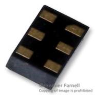
74LVC1T45GM - Brand New NXP Semiconductors Voltage Translators, Level Shifters
-
Description
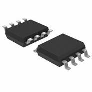
The 74LVC1T45GM is a voltage translator and level shifter electronic component model with a wide supply voltage range and high noise immunity capability, designed to enable bidirectional level translation. It features one data input-output port, a direction control input and dual supply pins, and both supply pins can be powered between 1.2 V and 5.5 V, which makes the device suitable for translating between any of the low voltage nodes like 1.2 V, 1.5 V, 1.8 V, 2.5 V, 3.3 V and 5.0 V. Additionally, the component is fully specified for partial power-down applications using IOFF, which provides partial Power-down mode operation.
Specifications and features
The following are the specifications and features of the 74LVC1T45GM model electronic component:
- Product Category: Voltage Translators, Level Shifters.
- Supply Voltage Range: VCC(A): 1.2 V to 5.5 V; VCC(B): 1.2 V to 5.5 V.
- Noise Immunity: High noise immunity.
- JEDEC Compliant: JESD8-7 (1.2 V to 1.95 V), JESD8-5 (1.8 V to 2.7 V), JESD8C (2.7 V to 3.6 V), JESD36 (4.5 V to 5.5 V).
- ESD Protection: HBM JESD22-A114E Class 3A exceeds 4000 V, CDM JESD22-C101C exceeds 1000 V.
- Maximum Data Rates: 420 Mbps (3.3 V to 5.0 V translation), 210 Mbps (translate to 3.3 V), 140 Mbps (translate to 2.5 V), 75 Mbps (translate to 1.8 V), 60 Mbps (translate to 1.5 V).
- Suspend Mode.
- Latch-up performance exceeds 100 mA per JESD 78 Class II.
- ±24 mA output drive (VCC = 3.0 V).
- Inputs accept voltages up to 5.5 V.
- Low power consumption: 16 μA maximum ICC.
- IOFF circuitry provides partial Power-down mode operation.
- Multiple package options.
Application Scenarios
The 74LVC1T45GM model electronic component can be used in various application scenarios, especially in situations that require bidirectional level translation and voltage shifting between low voltage nodes like 1.2 V, 1.5 V, 1.8 V, 2.5 V, 3.3 V, and 5.0 V. Some of its common application scenarios include:
- Signal conversion from I2C to SPI.
- Logic level shifting within battery management circuits.
- Keeping unused I/O pins in a known state in a mixed voltage system.
Comparison
Advantages- Wide supply voltage range, with both supply pins powering between 1.2 V and 5.5 V.
- High noise immunity, which ensures useful signal reception even in noisy environments.
- Complies with JEDEC standards, making it suitable for use with a wide range of devices.
- Has ESD protection capabilities that exceed 4000 V, which ensures it is resistant to electrostatic discharge.
- Low power consumption, which ensures power-efficient performance.
- IOFF circuitry that provides partial Power-down mode operation.
- Multiple package options.
Disadvantages- It has no obvious disadvantages.
-
Similar parts: 12 , Click to view
-
Datasheet
-
Shopping guide
Delivery period:
- - Will ship out in 2-3 days
- - DHL Express: 3-7 business days
- - DHL eCommerce: 12-22 business days
- - FedEx International Priority: 3-7 business days
- - EMS: 10-15 business days
Shipping fee:
- - Automatic Email notification (above 5 times)
- - View in your order page
Shipping option:
DHL, FedEx, EMS, SF Express, and Registered Air MailShipping tracking:
- - Automatic Email notification (above 5 times)
- - View in your order page
How to Buy:
- - In-stock, Add to cart > Check out > Submit order > Complete payment >Delivery.
- - Inquiry, Add to inquiry sheet/Submit bom/inquire file/Send email us > Quote > Place order > Complete payment >Delivery.
- View more
Payment:
- - Paypal,Credit Card includes Visa, Master, American Express.
- - Wire transfer, include Local bank transfer.
- - Western Union.
- View more
-
Popular parts of the same kind
- Datasheet: Download 74LVC1T45GM
- Chipdatas Part: CD86-74LVC1T45GM
- Warehouse: China, Hong Kong
- Dispatch: Within 24 hours
- Free Shipping: Yes
- Prority Shipping: Yes, 3-5 days
- Last Updated: 2024/10/01 07:56 +0800
-
- Full Refund if you don't receive your order
- Full or Partial Refund , If the item is not as described
-
 TXS0104EZXUR - Brand New Texas Instruments Voltage Translators, Level ShiftersBGA-12
 -
 100EP90 - Brand New ON Semiconductor Voltage Translators, Level ShiftersTSSOP-20
 -
 SY100ELT22LZITR - Brand New Microchip Technology Voltage Translators, Level Shifters8-SOIC 0.154", 3.90mm Width
 -
 TCA9406DCTR - Brand New Texas Instruments Voltage Translators, Level ShiftersMSOP-8
 -
 74AVCH2T45GT,115 - Brand New NXP Semiconductors Voltage Translators, Level Shifters8-XFDFN
 -
 ST4G3234BJR - Brand New STMicroelectronics Voltage Translators, Level Shifters11-WFBGA, FCBGA
 -
 TXB0104ZXUR - Brand New Texas Instruments Voltage Translators, Level Shifters12-UFBGA
 -
 TXB0104GXUR - Brand New Texas Instruments Voltage Translators, Level Shifters12-UFBGA
 -
 SN65LVELT22D - Brand New Texas Instruments Voltage Translators, Level Shifters8-SOIC 0.154", 3.90mm Width
 -
 NVT2002DP - Brand New NXP Semiconductors Voltage Translators, Level ShiftersTSSOP-8
-
The fee is charged according to the rule of PayPal.
-
The fee is charged according to the rule of PayPal.
-
Western Union charge US$0.00 banking fee.
-
We recommend to use bank transfer for large orders to save on handling fees.
-
DHL(www.dhl.com)
$40 limited time offer. -
UPS(www.ups.com)
$40 limited time offer. -
FedEx(www.fedex.com)
$40 limited time offer. -
Registered Mail(www.singpost.com)
Free shipping without minimum order.
