MX25L1635DM2I-12G - Brand New Macronix IC Chips
-
GENERAL DESCRIPTION
The MX25L1635D are 16,777,216 bit serial Flash memory, which is configured as 2,097,152 x 8 internally. When it is in two or four I/O read mode, the structure becomes 8,388,608 bits x 2 or 4,194,304 bits x 4. The MX25L1635D feature a serial peripheral interface and software protocol allowing operation on a simple 3-wire bus. The three bus signals are a clock input (SCLK), a serial data input (SI), and a serial data output (SO). Serial access to the device is enabled by CS# input.
When it is in two I/O read mode, the SI pin and SO pin become SIO0 pin and SIO1 pin for address/dummy bits input and data output. When it is in four I/O read mode, the SI pin, SO pin, WP# pin and NC pin become SIO0 pin, SIO1 pin, SIO2 pin and SIO3 pin for address/dummy bits input and data output.FEATURES
GENERAL
• Serial Peripheral Interface compatible -- Mode 0 and Mode 3
• 16M:16,777,216 x 1 bit structure or 8,388,608 x 2 bits (two I/O read mode) structure or 4,194,304 x 4 bits (four I/O read mode) structure
• 512 Equal Sectors with 4K byte each
- Any Sector can be erased individually
• 32 Equal Blocks with 64K byte each
- Any Block can be erased individually
• Single Power Supply Operation
- 2.7 to 3.6 volt for read, erase, and program operations
• Latch-up protected to 100mA from -1V to Vcc +1V
• Low Vcc write inhibit is from 1.5V to 2.5VPERFORMANCE
• High Performance
- Fast read
- 1 I/O: 104MHz & 86MHz with 8 dummy cycles
- 4 I/O: 75MHz with 6 dummy cycles
- 2 I/O: 75MHz with 4 dummy cycles
- Fast access time: 104MHz & 86MHz serial clock (15pF + 1TTL Load) and 66MHz serial clock (30pF + 1TTL Load)
- Serial clock of four I/O read mode : 75MHz (15pF + TTL Load), which is equivalent to 300MHz
- Fast program time: 1.4ms(typ.) and 5ms(max.)/page (256-byte per page)
- Byte program time: 9us (typical)
- Continuously program mode (automatically increase address under word program mode)
- Fast erase time: 60ms (typ.)/sector (4K-byte per sector) ; 0.7s(typ.) /block (64K-byte per block); 14s(typ.) /chip
• Low Power Consumption
- Low active read current: 25mA(max.) at 104MHz & 86MHz, 20mA(max.) at 66MHz and 10mA(max.) at 33MHz
- Low active programming current: 20mA (max.)
- Low active erase current: 20mA (max.)
- Low standby current: 20uA (max.)
• Typical 100,000 erase/program cycles
• 10 years data retentionSOFTWARE FEATURES
• Input Data Format
- 1-byte Command code
• Advanced Security Features
- Block lock protection
The BP0-BP3 status bit defines the size of the area to be software protection against program and erase instructions
- Additional 512-bit secured OTP for unique identifier
• Auto Erase and Auto Program Algorithm
- Automatically erases and verifies data at selected sector
- Automatically programs and verifies data at selected page by an internal algorithm that automatically times the program pulse widths (Any page to be programed should have page in the erased state first)
• Status Register Feature
• Electronic Identification
- JEDEC 1-byte manufacturer ID and 2-byte device ID
- RES command for 1-byte Device ID
- Both REMS,REMS2 and REMS4 commands for 1-byte manufacturer ID and 1-byte device IDHARDWARE FEATURES
• SCLK Input
- Serial clock input
• SI/SIO0
- Serial Data Input or Serial Data Input/Output for 2 x I/O read mode and 4 x I/O read mode
• SO/SIO1
- Serial Data Output or Serial Data Input/Output for 2 x I/O read mode and 4 x I/O read mode
• WP#/SIO2
- Hardware write protection or serial data Input/Output for 4 x I/O read mode
• NC/SIO3
- NC pin or serial data Input/Output for 4 x I/O read mode
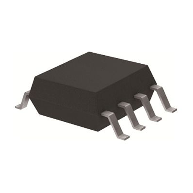
• PACKAGE
- 16-pin SOP (300mil)
- 8-land WSON (6x5mm)
- 8-pin SOP (200mil, 150mil)
- All Pb-free devices are RoHS Compliant -
Similar parts: 430483 , Click to view
-
Datasheet
-
Shopping guide
Delivery period:
- - Will ship out in 2-3 days
- - DHL Express: 3-7 business days
- - DHL eCommerce: 12-22 business days
- - FedEx International Priority: 3-7 business days
- - EMS: 10-15 business days
Shipping fee:
- - Automatic Email notification (above 5 times)
- - View in your order page
Shipping option:
DHL, FedEx, EMS, SF Express, and Registered Air MailShipping tracking:
- - Automatic Email notification (above 5 times)
- - View in your order page
How to Buy:
- - In-stock, Add to cart > Check out > Submit order > Complete payment >Delivery.
- - Inquiry, Add to inquiry sheet/Submit bom/inquire file/Send email us > Quote > Place order > Complete payment >Delivery.
- View more
Payment:
- - Paypal,Credit Card includes Visa, Master, American Express.
- - Wire transfer, include Local bank transfer.
- - Western Union.
- View more
-
Popular parts of the same kind
- Datasheet: Download MX25L1635DM2I-12G
- Chipdatas Part: CD86-MX25L1635DM2I-12G
- Warehouse: China, Hong Kong
- Dispatch: Within 24 hours
- Free Shipping: Yes
- Prority Shipping: Yes, 3-5 days
- Last Updated: 2024/06/28 22:51 +0800
-
- Full Refund if you don't receive your order
- Full or Partial Refund , If the item is not as described
-
 E-STLC2500CTR - Brand New STMicroelectronics IC ChipsWFBGA
 -
 CY7C68053A-56BA - Brand New Cypress Semiconductor IC ChipsBGA
 -
 AR8035-AL1A-R - Brand New QCA IC ChipsBGA
 -
 BL1117-ADC - Brand New Belling IC ChipsSOT-223
 -
 HM628512BLFP-7 - Brand New Nexperia IC ChipsSOP-32
 -
 BCM5325FKQMG - Brand New Broadcom IC ChipsQFP
 -
 D431000AGW-70LL - Brand New NEC IC ChipsSOP
 -
 HT46R003B - Brand New HOLTEK IC ChipsSOP-16
 -
 BCM2045KWBG - Brand New Broadcom IC ChipsBGA
 -
 H26M52103FMR - Brand New Skhynix IC ChipsBGA
-
The fee is charged according to the rule of PayPal.
-
The fee is charged according to the rule of PayPal.
-
Western Union charge US$0.00 banking fee.
-
We recommend to use bank transfer for large orders to save on handling fees.
-
DHL(www.dhl.com)
$40 limited time offer. -
UPS(www.ups.com)
$40 limited time offer. -
FedEx(www.fedex.com)
$40 limited time offer. -
Registered Mail(www.singpost.com)
Free shipping without minimum order.
