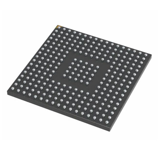
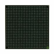
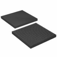
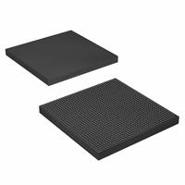
ORT8850L1BM680C - Brand New LATTICE FPGAs (Field Programmable Gate Array)
-
Introduction
Field-programmable system chips (FPSCs) bring a whole new dimension to programmable logic: FPGA logic and an embedded system solution on a single device. Agere Systems Inc. has developed a solution for designers who need the many advantages of FPGA-based design implementation, coupled with high-speed serial backplane data transfer.
Embedded Core Features (Serial)
■ Implemented in an ORCA Series 4 FPGA.
■ Allows wide range of applications for SONET network termination application as well as generic data moving for high-speed backplane data transfer.
■ No knowledge of SONET/SDH needed in generic applications. Simply supply data, 78 MHz—106 MHz clock, and a frame pulse.
■ High-speed interface (HSI) function for clock/data recovery serial backplane data transfer without external clocks.
■ Eight-channel HSI function provides 850 Mbits/s serial interface per channel for a total chip bandwidth of 6.8 Gbits/s (full duplex).
■ HSI function uses Agere’s 850 Mbits/s serial interface core. Rates from 212 Mbits/s to 850 Mbits/s are supported directly (lower rates directly supported through decimation and interpolation).
■ LVDS I/Os compliant with EIA®-644 support hot insertion. All embedded LVDS I/Os include both input and output on-board termination to allow long-haul driving of backplanes.
■ Low-power 1.5 V HSI core.
■ Low-power LVDS buffers.
■ Programmable STS-1, STS-3, and STS-12 framing.
■ Independent STS-1, STS-3, and STS-12 data streams per quad channels.
■ 8:1 data multiplexing/demultiplexing for 106.25 MHz byte-wide data processing in FPGA logic.
■ On-chip, phase-lock loop (PLL) clock meets B jitter tolerance specification of ITU-T recommendation G.958.
■ Powerdown option of HSI receiver on a per-channel basis.
■ Selectable 8B/10B coder/decoder or SONET scrambler/descrambler.
■ HSI automatically recovers from loss-of-clock once its reference clock returns to normal operating state.
■ Frame alignment across multiple ORT8850 devices for work/protect switching at OC-192/STM-64 and above rates.
■ In-band management and configuration through transport overhead extraction/insertion.
■ Supports transparent modes where either the only insertion is A1/A2 framing bytes, or no bytes are inserted.
■ Streamlined pointer processor (pointer mover) for 8 kHz frame alignment to system clocks.
■ Built-in boundry scan (IEEE ®1149.1 JTAG).
■ FIFOs align incoming data across all eight channels (two groups of four channels or four groups of two channels) for both SONET scrambling and 8B/10B modes. Optional ability to bypass alignment FIFOs.
■ 1 + 1 protection supports STS-12/STS-48 redundancy by either software or hardware control for protection switching applications. STS-192 and above rates are supported through multiple devices.
■ ORCA FPGA soft intellectual property core support for a variety of applications.
■ Programmable STM pointer mover bypass mode.
■ Programmable STM framer bypass mode.
■ Programmable CDR bypass mode (clocked LVDS high-speed interface).
■ Redundant outputs and multiplexed redundant inputs for CDR I/Os allow for implementation of eight channels with redundancy on a single device. -
ähnliche Teile: 3140 , Klicke zum Zeigen
-
Datenblatt
-
Shopping guide
Delivery period:
- - Will ship out in 2-3 days
- - DHL Express: 3-7 business days
- - DHL eCommerce: 12-22 business days
- - FedEx International Priority: 3-7 business days
- - EMS: 10-15 business days
Shipping fee:
- - Automatic Email notification (above 5 times)
- - View in your order page
Shipping option:
DHL, FedEx, EMS, SF Express, and Registered Air MailShipping tracking:
- - Automatic Email notification (above 5 times)
- - View in your order page
How to Buy:
- - In-stock, Add to cart > Check out > Submit order > Complete payment >Delivery.
- - Inquiry, Add to inquiry sheet/Submit bom/inquire file/Send email us > Quote > Place order > Complete payment >Delivery.
- View more
Payment:
- - Paypal,Credit Card includes Visa, Master, American Express.
- - Wire transfer, include Local bank transfer.
- - Western Union.
- View more
- Datasheet: Download ORT8850L1BM680C
- Chipdaten Teil: CD86-ORT8850L1BM680C
- Lagerhaus: China, Hongkong
- Versenden: Innerhalb von 24 Stunden
- Kostenloser Versand: Yes
- Bevorzugter Versand: Yes, 3-5 days
- Letzte Aktualisierung: 2024/06/29 05:22 +0800
-
- Vollständige Rückerstattung, wenn Sie Ihre Bestellung nicht erhalten
- Vollständige oder teilweise Rückerstattung, wenn der Artikel nicht der Beschreibung entspricht
-
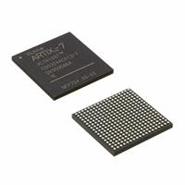 XC6SLX45-3CSG324I - Brand New XILINX FPGAs (Field Programmable Gate Array)CSBGA-324
 -
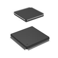 APA075-PQG208 - Brand New Microchip Technology FPGAs (Field Programmable Gate Array)208-BFQFP
 -
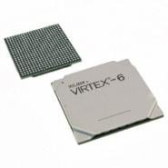 XC6VLX130T-1FFG784C - Brand New XILINX FPGAs (Field Programmable Gate Array)784-BBGA, FCBGA
 -
 XC4VFX20-11FFG672I - Brand New XILINX FPGAs (Field Programmable Gate Array)672-BBGA, FCBGA
 -
 EP2S60F672I4N - Brand New Intel / Altera FPGAs (Field Programmable Gate Array)672-BBGA, FCBGA
 -
 XC4VFX100-10FFG1517C - Brand New XILINX FPGAs (Field Programmable Gate Array)1517-BBGA, FCBGA
 -
 EP3C40F484C6N - Brand New Intel / Altera FPGAs (Field Programmable Gate Array)484-BGA
 -
 LFXP3C-3TN144C - Brand New Lattice Semiconductor FPGAs (Field Programmable Gate Array)144-LQFP
 -
 XCV50-4FG256C - Brand New XILINX FPGAs (Field Programmable Gate Array)256-BGA
 -
 EP4CE30F23C8N - Brand New Intel / Altera FPGAs (Field Programmable Gate Array)BGA
-
Die Gebühr wird gemäß der PayPal-Regel erhoben.
-
Die Gebühr wird gemäß der PayPal-Regel erhoben.
-
Western Union erhebt eine Bankgebühr von 0,00 US-Dollar.
-
Wir empfehlen, bei größeren Bestellungen die Banküberweisung zu nutzen, um Bearbeitungsgebühren zu sparen.
-
DHL(www.dhl.com)
Zeitlich begrenztes Angebot im Wert von 40 $. -
UPS(www.ups.com)
Zeitlich begrenztes Angebot im Wert von 40 $. -
FedEx(www.fedex.com)
Zeitlich begrenztes Angebot im Wert von 40 $. -
Registered Mail(www.singpost.com)
Kostenloser Versand ohne Mindestbestellwert.
