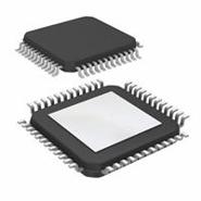
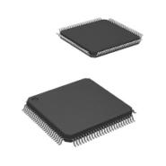
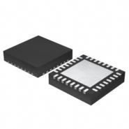
MM912F634CV1AE - Brand New Freescale / NXP Application Specific Microcontrollers
-
Description
The MM912F634CV1AE is an application-specific microcontroller designed to provide a combined solution for HCS12 microcontroller and SMARTMOS analog control IC. This electronic component integrates system base chips and application-specific functions, with a LIN transceiver. The device consists of 16-bit S12 CPU, 32kByte flash, and 2.0kByte RAM. It includes background debug and a debug module, providing a die to die (D2D) bus interface for transparent memory mapping. The device has a LIN 2.1 Physical Layer interface with an integrated SCI, six digital MCU GPIOs shared with SPI, a 10-bit 15 channel Analog to Digital converter, and a 16-bit 4 channel timer module.
Specifications and features
- 16-Bit S12 CPU, 32 kByte FLASH, 2.0 kByte RAM
- Background Debug (BDM) & Debug Module (DBG)
- Die to Die bus interface for transparent memory mapping
- On-chip oscillator & two independent watchdogs
- LIN 2.1 Physical Layer Interface with integrated SCI
- Six digital MCU GPIOs shared with SPI (PA5…0)
- 10-Bit, 15 Channel- Analog to Digital Converter (ADC)
- 16-Bit, 4 Channel- Timer Module (TIM16B4C)
- 8-Bit, 2 Channel- Pulse width modulation module (PWM)
- Six high-voltage / Wake-up inputs (L5.0)
- Three low voltage GPIOs (PB2.0)
- Low Power Modes with cyclic sense & forced wake-up
- Current Sense Module with selectable gain
- Reverse Battery protected Voltage Sense Module
- Two protected low side outputs to drive inductive loads
- Two protected high side outputs
- Chip temperature sensor
- Hall sensor supply
- Integrated voltage regulator(s)
Application Scenarios
The MM912F634CV1AE is widely used in the automotive industry for electric motor drives, battery management, and for the intelligent power distribution system.
Comparison
Advantages- Integration of HCS12 microcontroller with SMARTMOS analog control IC
- The device consists of 16-bit S12 CPU, 32kByte flash, and 2.0kByte RAM
- LIN 2.1 Physical Layer interface with an integrated SCI
- Die to Die (D2D) bus interface for transparent memory mapping
- Low Power Modes with cyclic sense & forced wake-up
- Wide application in the automotive industry
Disadvantages- This chip doesn't support Wi-Fi and Bluetooth connectivity.
- The 16-bit architecture may not work efficiently with processor-heavy applications.
-
Similar parts: 216 , Click to view
-
Datasheet
-
Shopping guide
Delivery period:
- - Will ship out in 2-3 days
- - DHL Express: 3-7 business days
- - DHL eCommerce: 12-22 business days
- - FedEx International Priority: 3-7 business days
- - EMS: 10-15 business days
Shipping fee:
- - Automatic Email notification (above 5 times)
- - View in your order page
Shipping option:
DHL, FedEx, EMS, SF Express, and Registered Air MailShipping tracking:
- - Automatic Email notification (above 5 times)
- - View in your order page
How to Buy:
- - In-stock, Add to cart > Check out > Submit order > Complete payment >Delivery.
- - Inquiry, Add to inquiry sheet/Submit bom/inquire file/Send email us > Quote > Place order > Complete payment >Delivery.
- View more
Payment:
- - Paypal,Credit Card includes Visa, Master, American Express.
- - Wire transfer, include Local bank transfer.
- - Western Union.
- View more
-
Popular parts of the same kind
- Datasheet: Download MM912F634CV1AE
- Chipdatas Part: CD91-MM912F634CV1AE
- Warehouse: China, Hong Kong
- Dispatch: Within 24 hours
- Free Shipping: Yes
- Prority Shipping: Yes, 3-5 days
- Last Updated: 2024/09/30 10:37 +0800
-
- Full Refund if you don't receive your order
- Full or Partial Refund , If the item is not as described
-
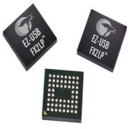
 CY7C68013A-56LTXC - Brand New Cypress Semiconductor Application Specific MicrocontrollersQFN
 -
 CYUSB3314-88LTXI - Brand New Cypress Semiconductor Application Specific Microcontrollers88-VFQFN Exposed Pad
 -
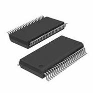
 CY7C68013A-56PVXI - Brand New Cypress Semiconductor Application Specific MicrocontrollersSSOP
 -
 AT43USB370E-AC - Brand New Intel / Altera Application Specific Microcontrollers100-LQFP
 -
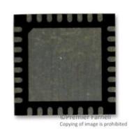 CY8C20436A-24LQ - Brand New Cypress Semiconductor Application Specific MicrocontrollersQFN
 -
 CYUSB3304-68LTXC - Brand New Cypress Semiconductor Application Specific MicrocontrollersQFN
 -
 CY7C66013C-PVXC - Brand New Cypress Semiconductor Application Specific Microcontrollers48-BSSOP 0.295", 7.50mm Width
 -
 CY7C68013A-56BA - Brand New Cypress Semiconductor Application Specific MicrocontrollersBGA
 -
 CY8C20446A-24LQ - Brand New Cypress Semiconductor Application Specific MicrocontrollersQFN-32
 -
 CY7C63221A-PC - Brand New Cypress Semiconductor Application Specific Microcontrollers16-DIP 0.300", 7.62mm
-
The fee is charged according to the rule of PayPal.
-
The fee is charged according to the rule of PayPal.
-
Western Union charge US$0.00 banking fee.
-
We recommend to use bank transfer for large orders to save on handling fees.
-
DHL(www.dhl.com)
$40 limited time offer. -
UPS(www.ups.com)
$40 limited time offer. -
FedEx(www.fedex.com)
$40 limited time offer. -
Registered Mail(www.singpost.com)
Free shipping without minimum order.
