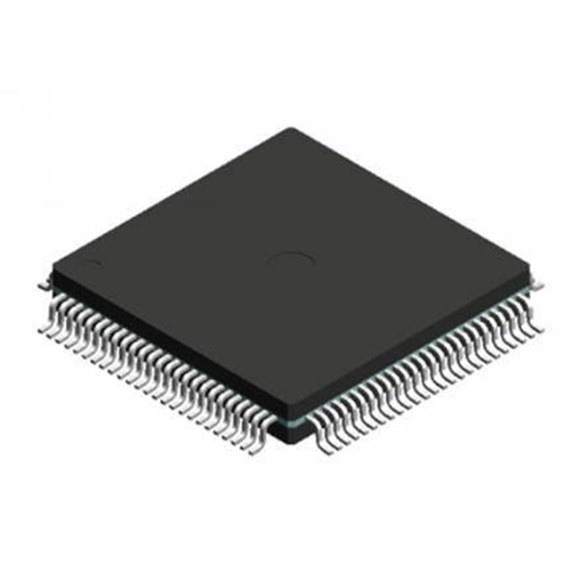
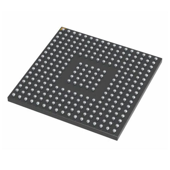
OR2C26A-4PS240 - Brand New Lattice Semiconductor IC Chips
-
Description
The ORCA Series 2 series of SRAM-based FPGAs, model OR2C26A-4PS240, is an enhanced version of the ATT2C/2T architecture. It includes patented architectural enhancements that make functions faster and easier to design while conserving the use of PLCs and routing resources.
Specifications and features
- High-performance, cost-effective, low-power 0.35 µm CMOS technology (OR2CxxA), 0.3 µm CMOS technology (OR2TxxA), and 0.25 µm CMOS technology (OR2TxxB), (four-input look-up table (LUT) delay less than 1.0 ns with -8 speed grade)
- High density (up to 43,200 usable, logic-only gates; or 99,400 gates including RAM)
- Up to 480 user I/Os (OR2TxxA and OR2TxxB I/Os are 5 V tolerant to allow interconnection to both 3.3 V and 5 V devices, selectable on a per-pin basis)
- Four 16-bit look-up tables and four latches/flip-flops per PFU, nibble-oriented for implementing 4-, 8-, 16-, and/or 32-bit (or wider) bus structures
- Eight 3-state buffers per PFU for on-chip bus structures
- Fast, on-chip user SRAM has features to simplify RAM design and increase RAM speed:
- Asynchronous single port: 64 bits/PFU
- Synchronous single port: 64 bits/PFU
- Synchronous dual port: 32 bits/PFU
- Improved ability to combine PFUs to create larger RAM structures using write-port enable and 3-state buffers
- Fast, dense multipliers can be created with the multiplier mode (4 x 1 multiplier/PFU):
- 8 x 8 multiplier requires only 16 PFUs
- 30% increase in speed
- Flip-flop/latch options to allow programmable priority of synchronous set/reset vs. clock enable
- Enhanced cascadable nibble-wide data path capabilities for adders, subtractors, counters, multipliers, and comparators including internal fast-carry operation
- Innovative, abundant, and hierarchical nibbleoriented routing resources that allow automatic use of internal gates for all device densities without sacrificing performance
- Upward bit stream compatible with the ORCA ATT2Cxx/ATT2Txx series of devices
- Pinout-compatible with new ORCA Series 3 FPGAs
- TTL or CMOS input levels programmable per pin for the OR2CxxA (5 V) devices
- Individually programmable drive capability: 12 mA sink/6 mA source or 6 mA sink/3 mA source
- Built-in boundary scan (IEEE 1149.1 JTAG) and 3-state all I/O pins, (TS_ALL) testability functions
- Multiple configuration options, including simple, low pincount serial ROMs, and peripheral or JTAG modes for in-system programming (ISP)
- Full PCI bus compliance for all devices
- Supported by industry-standard CAE tools for design entry, synthesis, and simulation with ORCA Foundry Development System support (for back-end implementation)
- New, added features (OR2TxxB) have:
- More I/O per package than the OR2TxxA family
- No dedicated 5 V supply (VDD5)
- Faster configuration speed (40 MHz)
- Pin selectable I/O clamping diodes provide 5V or 3.3V PCI compliance and 5V tolerance
- Full PCI bus compliance in both 5V and 3.3V PCI systems
IEEE is a registered trademark of The Institute of Electrical and Electronics Engineers, Inc.
Application Scenarios
The ORCA Series 2 FPGAs are commonly used in various electronic applications that require high-performance and low-power consumption. These applications include:
- Communication equipment
- Data processing systems
- Industrial control systems
- Automotive electronics
- Medical devices
- And many more
Comparison
The ORCA Series 2 FPGAs offer several advantages over other similar models:
- Enhanced architecture for faster and easier design
- High-performance and low-power consumption
- High density with up to 43,200 usable gates
- Support for a large number of user I/Os
- Flexible configuration options for in-system programming
- Compatibility with industry-standard CAE tools
- Pinout compatibility with new ORCA Series 3 FPGAs
However, there are a few disadvantages to consider:
- Requires knowledge and expertise in FPGA design
- Cost may be higher compared to less advanced models
-
Similar parts: 430483 , Click to view
-
Datasheet
-
Shopping guide
Delivery period:
- - Will ship out in 2-3 days
- - DHL Express: 3-7 business days
- - DHL eCommerce: 12-22 business days
- - FedEx International Priority: 3-7 business days
- - EMS: 10-15 business days
Shipping fee:
- - Automatic Email notification (above 5 times)
- - View in your order page
Shipping option:
DHL, FedEx, EMS, SF Express, and Registered Air MailShipping tracking:
- - Automatic Email notification (above 5 times)
- - View in your order page
How to Buy:
- - In-stock, Add to cart > Check out > Submit order > Complete payment >Delivery.
- - Inquiry, Add to inquiry sheet/Submit bom/inquire file/Send email us > Quote > Place order > Complete payment >Delivery.
- View more
Payment:
- - Paypal,Credit Card includes Visa, Master, American Express.
- - Wire transfer, include Local bank transfer.
- - Western Union.
- View more
-
Popular parts of the same kind
- Datasheet: Download OR2C26A-4PS240
- Chipdatas Part: CD93-OR2C26A-4PS240
- Warehouse: China, Hong Kong
- Dispatch: Within 24 hours
- Free Shipping: Yes
- Prority Shipping: Yes, 3-5 days
- Last Updated: 2024/06/03 15:52 +0800
-
- Full Refund if you don't receive your order
- Full or Partial Refund , If the item is not as described
-
The fee is charged according to the rule of PayPal.
-
The fee is charged according to the rule of PayPal.
-
Western Union charge US$0.00 banking fee.
-
We recommend to use bank transfer for large orders to save on handling fees.
-
DHL(www.dhl.com)
$40 limited time offer. -
UPS(www.ups.com)
$40 limited time offer. -
FedEx(www.fedex.com)
$40 limited time offer. -
Registered Mail(www.singpost.com)
Free shipping without minimum order.
