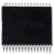
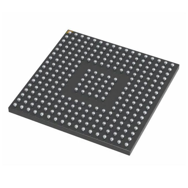
-
DESCRIPTION
The PM8315 High Density T1/E1 Framer with Integrated VT/TU Mapper and M13 Multiplexer (TEMUX) is a feature-rich device for use in any applications requiring high density link termination over T1 channelized DS3 or T1 and E1 channelized SONET/SDH facilities.
FEATURES
• Integrates 28 T1 framers, 21 E1 framers, a SONET/SDH VT1.5/VT2/TU11/TU12 bit asynchronous mapper, a full featured M13 multiplexer with DS3 framer, and a SONET/SDH DS3 mapper in a single monolithic device for terminating DS3 multiplexed T1 streams, SONET/SDH mapped T1 streams or SONET/SDH mapped E1 streams.
• Seven T1 modes of operation:
• Up to 28 T1 streams mapped as bit asynchronous VT1.5 virtual tributaries into a STS-1 SPE or TU-11 tributary units into a STM-1/VC3 or TU-11 tributary units into a TUG3 in a STM-1/VC4.
• Single STS-1, AU3 or TUG3 Bit Asynchronous VT1.5 or TU-11 Mapper with ingress or egress per tributary link monitoring.
• Up to 28 T1 streams M13 multiplexed into a serial DS3.
• Up to 28 T1 streams M13 multiplexed into a DS3, the DS3 is asynchronously mapped into a STS-1 SPE.
• DS3 M13 Multiplexer with ingress or egress per link monitoring.
• Up to 28 DS3 multiplexed T1 streams are mapped as bit asynchronous VT1.5 virtual tributaries or TU-11 tributary units, providing a transmultiplexing (“transmux”) function between DS3 and SONET/SDH.
• Up to 21 T1 streams mapped as bit asynchronous TU-12 tributary units into a STM-1/VC3 or TUG3 from a STM-1/VC4.
• Three E1 modes of operation:
• Up to 21 E1 streams mapped as bit asynchronous VT2 virtual tributaries into a STS-1 SPE or TU-12 tributary units into a STM-1/VC3 or TUG3 from a STM-1/VC4.
• Single STS-1, AU3 or TUG3 Bit Asynchronous VT2 or TU-12 Mapper with ingress or egress per tributary link monitoring.
• Up to 21 E1 streams multiplexed into a DS3 following the ITU-T G.747 recommendation. This E1 mode of operation is restricted to using the serial clock and data or HMVIP system interfaces.
• Provides an HDLC interface with 128 bytes of buffering for terminating the
facility data link.
• Provides performance monitoring counters sufficiently large as to allow performance monitor counter polling at a minimum rate of once per second. Optionally, updates the performance monitoring counters and interrupts the microprocessor once per second, timed to the receive line.
• Provides an optional elastic store which may be used to time the ingress streams to a common clock and frame alignment, or to facilitate per-DS0 loopbacks.
• Provides DS-1 robbed bit signaling extraction, with optional data inversion, programmable idle code substitution, digital milliwatt code substitution, bit fixing, and two superframes of signaling debounce on a per-channel basis.
• A pseudo-random sequence user selectable from 211 –1, 215 –1 or220 –1, may be detected in the T1 stream in either the ingress or egress directions. The detector counts pattern errors using a 24-bit non-saturating PRBS error counter. The pseudo-random sequence can be the entire T1 or any combination of DS0s within a framed T1.
• Line side interface is either from the DS3 interface via the M13 multiplex or from the SONET/SDH Drop bus via the VT1.5, TU-11, VT2 or TU-12 demapper.
• System side interface is either serial clock and data, MVIP or SBI bus.
• Frames in the presence of and detects the “Japanese Yellow” alarm.Each one of 21 E1 receiver sections:
• Provides external access for up to two de-jittered recovered T1 clocks.
• Frames to ITU-T G.704 basic and CRC-4 multiframe formatted E1 signals. The framing procedures are consistent ITU-T G.706 specifications.
• Provides an HDLC interface with 128 bytes of buffering for terminating the national use bit data link.
• Extracts 4-bit codewords from the E1 national use bits as specified in ETS 300 233.
• V5.2 link indication signal detection.
• Provides a digital phase locked loop for generation of a low jitter transmit clock.
• Provides a FIFO buffer for jitter attenuation and rate conversion in the transmitter.
• Automatically generates and transmits DS-1 performance report messages to ANSI T1.231and ANSI T1.408 specifications.
• Supports the alternate ESF CRC-6 calculation for Japanese applications.
• A pseudo-random sequence user selectable from 211 –1, 215 –1 or 220 –1, may be inserted into the T1 stream in either the ingress or egress directions. The pseudo-random sequence can be inserted into the entire T1 or any combination of DS0s within the framed T1.
• Line side interface is through either DS3 Interface via the M13 multiplex or the SONET/SDH Add bus via the VT1.5, TU-11, VT2 or TU-12 mapper.
• System side interface is either serial clock and data, MVIP or SBI bus.APPLICATIONS
• High density T1 interfaces for multiplexers, multi-service switches, routers and digital modems.
• High density E1 interfaces for multiplexers, multi-service switches, routers and digital modems.
• Frame Relay switches and access devices (FRADS)
• SONET/SDH Add Drop Multiplexers
• SONET/SDH Terminal Multiplexers
• M23 Based M13 Multiplexer
• C-Bit Parity Based M13 Multiplexer
• Channelized and Unchannelized DS3 Frame Relay Interfaces -
Similar parts: 430483 , Click to view
-
Datasheet
-
Shopping guide
Delivery period:
- - Will ship out in 2-3 days
- - DHL Express: 3-7 business days
- - DHL eCommerce: 12-22 business days
- - FedEx International Priority: 3-7 business days
- - EMS: 10-15 business days
Shipping fee:
- - Automatic Email notification (above 5 times)
- - View in your order page
Shipping option:
DHL, FedEx, EMS, SF Express, and Registered Air MailShipping tracking:
- - Automatic Email notification (above 5 times)
- - View in your order page
How to Buy:
- - In-stock, Add to cart > Check out > Submit order > Complete payment >Delivery.
- - Inquiry, Add to inquiry sheet/Submit bom/inquire file/Send email us > Quote > Place order > Complete payment >Delivery.
- View more
Payment:
- - Paypal,Credit Card includes Visa, Master, American Express.
- - Wire transfer, include Local bank transfer.
- - Western Union.
- View more
-
Popular parts of the same kind
- Datasheet: Download PM8303A-WGI
- Chipdatas Part: CD94-PM8303A-WGI
- Warehouse: China, Hong Kong
- Dispatch: Within 24 hours
- Free Shipping: Yes
- Prority Shipping: Yes, 3-5 days
- Last Updated: 2024/06/03 09:24 +0800
-
- Full Refund if you don't receive your order
- Full or Partial Refund , If the item is not as described
-
The fee is charged according to the rule of PayPal.
-
The fee is charged according to the rule of PayPal.
-
Western Union charge US$0.00 banking fee.
-
We recommend to use bank transfer for large orders to save on handling fees.
-
DHL(www.dhl.com)
$40 limited time offer. -
UPS(www.ups.com)
$40 limited time offer. -
FedEx(www.fedex.com)
$40 limited time offer. -
Registered Mail(www.singpost.com)
Free shipping without minimum order.
