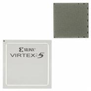
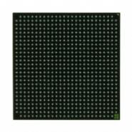
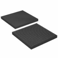
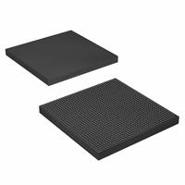
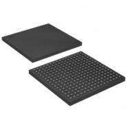
XC5VLX1552FFG1153I - Brand New XC FPGAs (Field Programmable Gate Array)
-
Description
The XC5VLX1552FFG1153I is a high-performance FPGA (Field Programmable Gate Array) component. It is a member of the XC5VLX1552FFG1153I family and is specifically designed for wireless infrastructure applications that require general filtering operations. The component features a powerful on-chip enhanced filter coprocessor (EFCOP) that processes filter algorithms in parallel with core operations, resulting in increased overall DSP performance and efficiency. With a high-performance, single-clock-cycle-per-instruction engine and a 24-bit addressing capability, the XC5VLX1552FFG1153I offers exceptional performance at 100 million instructions per second (MIPS) using an internal 100 MHz clock. It operates at a core voltage of 2.5 volts and has separate 3.3 volt input/output power.
Specifications and features
- High-Performance DSP56300 Core - 100 million instructions per second (MIPS) with a 100 MHz clock at 2.5 V core and 3.3 V I/O - Object code compatible with the DSP56000 core - Highly parallel instruction set - Data arithmetic logic unit (ALU) with a fully pipelined 24 x 24-bit parallel multiplier-accumulator - 56-bit parallel barrel shifter for fast shift and normalization, bit stream generation and parsing - Conditional ALU instructions - 24-bit or 16-bit arithmetic support under software control - Program control unit (PCU) with position independent code (PIC) support, optimized addressing modes for DSP applications, on-chip instruction cache controller, on-chip memory-expandable hardware stack, nested hardware DO loops, and fast auto-return interrupts - Direct memory access (DMA) with support for six channels, one-, two-, and three-dimensional transfers, end-of-block-transfer interrupts, and triggering from interrupt lines and all peripherals - Phase-locked loop (PLL) that allows change of low power divide factor (DF) without loss of lock and provides an output clock with skew elimination - Hardware debugging support with On-Chip Emulation (OnCE) module and Joint Test Action Group (JTAG) test access port (TAP) - Address trace mode that reflects internal Program RAM accesses at the external port
Application Scenarios
The XC5VLX1552FFG1153I FPGA component is ideal for use in wireless infrastructure applications that require general filtering operations. It can be used in various scenarios, including wireless communication systems, base station equipment, signal processing applications, and more. With its high-performance capabilities and efficient processing power, it provides a reliable solution for demanding applications in the wireless industry.
Comparison
Advantages- High-performance DSP56300 core with 100 million instructions per second (MIPS) capability - Highly parallel instruction set and efficient data arithmetic logic unit (ALU) - Versatile program control unit (PCU) with optimized addressing modes and on-chip memory-expandable hardware stack - Direct memory access (DMA) with multiple channels and support for different types of transfers - Phase-locked loop (PLL) for flexible clock generation and skew elimination - On-chip emulation (OnCE) module and JTAG test access port (TAP) for hardware debugging support - Address trace mode for monitoring internal Program RAM accesses
Disadvantages- Requires separate power for core and input/output (I/O) - Limited support for specific application scenarios outside of wireless infrastructure applications
-
Similar parts: 3140 , Click to view
-
Datasheet
-
Shopping guide
Delivery period:
- - Will ship out in 2-3 days
- - DHL Express: 3-7 business days
- - DHL eCommerce: 12-22 business days
- - FedEx International Priority: 3-7 business days
- - EMS: 10-15 business days
Shipping fee:
- - Automatic Email notification (above 5 times)
- - View in your order page
Shipping option:
DHL, FedEx, EMS, SF Express, and Registered Air MailShipping tracking:
- - Automatic Email notification (above 5 times)
- - View in your order page
How to Buy:
- - In-stock, Add to cart > Check out > Submit order > Complete payment >Delivery.
- - Inquiry, Add to inquiry sheet/Submit bom/inquire file/Send email us > Quote > Place order > Complete payment >Delivery.
- View more
Payment:
- - Paypal,Credit Card includes Visa, Master, American Express.
- - Wire transfer, include Local bank transfer.
- - Western Union.
- View more
- Datasheet: Download XC5VLX1552FFG1153I
- Chipdatas Part: CD87-XC5VLX1552FFG1153I
- Warehouse: China, Hong Kong
- Dispatch: Within 24 hours
- Free Shipping: Yes
- Prority Shipping: Yes, 3-5 days
- Last Updated: 2024/06/03 10:33 +0800
-
- Full Refund if you don't receive your order
- Full or Partial Refund , If the item is not as described
-
 XC6SLX45-3CSG324I - Brand New XILINX FPGAs (Field Programmable Gate Array)CSBGA-324
 -
 APA075-PQG208 - Brand New Microchip Technology FPGAs (Field Programmable Gate Array)208-BFQFP
 -
 XC6VLX130T-1FFG784C - Brand New XILINX FPGAs (Field Programmable Gate Array)784-BBGA, FCBGA
 -
 XC4VFX20-11FFG672I - Brand New XILINX FPGAs (Field Programmable Gate Array)672-BBGA, FCBGA
 -
 EP2S60F672I4N - Brand New Intel / Altera FPGAs (Field Programmable Gate Array)672-BBGA, FCBGA
 -
 XC4VFX100-10FFG1517C - Brand New XILINX FPGAs (Field Programmable Gate Array)1517-BBGA, FCBGA
 -
 EP3C40F484C6N - Brand New Intel / Altera FPGAs (Field Programmable Gate Array)484-BGA
 -
 LFXP3C-3TN144C - Brand New Lattice Semiconductor FPGAs (Field Programmable Gate Array)144-LQFP
 -
 XCV50-4FG256C - Brand New XILINX FPGAs (Field Programmable Gate Array)256-BGA
 -
 EP4CE30F23C8N - Brand New Intel / Altera FPGAs (Field Programmable Gate Array)BGA
-
The fee is charged according to the rule of PayPal.
-
The fee is charged according to the rule of PayPal.
-
Western Union charge US$0.00 banking fee.
-
We recommend to use bank transfer for large orders to save on handling fees.
-
DHL(www.dhl.com)
$40 limited time offer. -
UPS(www.ups.com)
$40 limited time offer. -
FedEx(www.fedex.com)
$40 limited time offer. -
Registered Mail(www.singpost.com)
Free shipping without minimum order.
