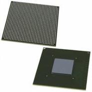
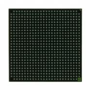
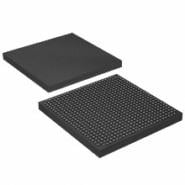
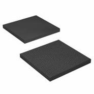
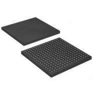
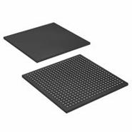
EP2AGX260FF35C5N - Brand New Intel / Altera FPGAs (Field Programmable Gate Array)
-
Description
[ ALTERA ]
Electronic Component Model:EP2AGX260FF35C5N
Product Category:FPGAs (Field Programmable Gate Array)
The Arria® II device family is designed specifically for ease-of-use. The cost-optimized, 40-nm device family architecture features a low-power, programmable logic engine and streamlined transceivers and I/Os. Common interfaces, such as the Physical Interface for PCI Express® (PCIe®), Ethernet, and DDR3 memory are easily implemented in your design with the Quartus® II software, the SOPC Builder design software, and a broad library of hard and soft intellectual property (IP) solutions from Altera. The Arria II device family makes designing for applications requiring transceivers operating at up to 6.375 Gbps fast and easy.
Specifications and features
The Arria II device features consist of the following highlights:
■ 40-nm, low-power FPGA engine
■ Adaptive logic module (ALM) offers the highest logic efficiency in the industry
■ Eight-input fracturable look-up table (LUT)
■ Memory logic array blocks (MLABs) for efficient implementation of small FIFOs
■ High-performance digital signal processing (DSP) blocks up to 550 MHz
■ Configurable as 9 x 9-bit, 12 x 12-bit, 18 x 18-bit, and 36 x 36-bit full- precision multipliers as well as 18 x 36-bit high-precision multiplier
■ Hardcoded adders, subtractors, accumulators, and summation functions
■ Fully-integrated design flow with the MATLAB and DSP Builder software from Altera
■ Maximum system bandwidth
■ Up to 24 full-duplex clock data recovery (CDR)-based transceivers supporting rates between 600 Mbps and 6.375 Gbps
■ Dedicated circuitry to support physical layer functionality for popular serial
protocols, including PCIe Gen1 and PCIe Gen2, Gbps Ethernet, Serial
RapidIO® (SRIO), Common Public Radio Interface (CPRI), OBSAI,
SD/HD/3G/ASI Serial Digital Interface (SDI), XAUI and Reduced XAUI
(RXAUI), HiGig/HiGig+, SATA/Serial Attached SCSI (SAS), GPON,
SerialLite II, Fiber Channel, SONET/SDH, Interlaken, Serial Data Converter
(JESD204), and SFI-5.
■ Complete PIPE protocol solution with an embedded hard IP block that provides physical interface and media access control (PHY/MAC) layer, Data Link layer, and Transaction layer functionality
■ Optimized for high-bandwidth system interfaces
■ Up to 726 user I/O pins arranged in up to 20 modular I/O banks that support a wide range of single-ended and differential I/O standards
■ High-speed LVDS I/O support with serializer/deserializer (SERDES) and dynamic phase alignment (DPA) circuitry at data rates from 150 Mbps to 1.25 Gbps
■ Low power
■ Architectural power reduction techniques
■ Typical physical medium attachment (PMA) power consumption of 100 mW at 3.125 Gbps.
■ Power optimizations integrated into the Quartus II development software
■ Advanced usability and security features
■ Parallel and serial configuration options
■ On-chip series (RS) and on-chip parallel (RT) termination with auto- calibration for single-ended I/Os and on-chip differential (RD) termination for differential I/O
■ 256-bit advanced encryption standard (AES) programming file encryption for design security with volatile and non-volatile key storage options
■ Robust portfolio of IP for processing, serial protocols, and memory interfaces
■ Low cost, easy-to-use development kits featuring high-speed mezzanine connectors (HSMC)
■ Emulated LVDS output support with a data rate of up to 1152 MbpsApplication Scenarios
The Arria II device family is commonly used in applications requiring transceivers operating at up to 6.375 Gbps. It is designed for ease-of-use and features a low-power, programmable logic engine and streamlined transceivers and I/Os. The device family is compatible with common interfaces such as PCIe, Ethernet, and DDR3 memory, making it versatile for various design applications. With the Quartus II software and a library of IP solutions, designing with the Arria II device family is fast and efficient.
Comparison
Advantages:
- Cost-optimized, low-power architecture
- High logic efficiency with the Adaptive Logic Module (ALM)
- Efficient implementation of small FIFOs with Memory Logic Array Blocks (MLABs)
- High-performance digital signal processing (DSP) blocks
- Configurable as various precision multipliers
- Fully-integrated design flow with MATLAB and DSP Builder software
- Supports a wide range of system interfaces
- Large number of user I/O pins for flexible design
- Low power consumption
- Advanced usability and security features
- Robust portfolio of IP for processing, serial protocols, and memory interfaces
- Easy-to-use development kits
- Emulated LVDS output support
Disadvantages:
- Limited to specific applications requiring transceivers operating at up to 6.375 Gbps
- Requires Quartus II software for design implementation
- May have a learning curve for beginners in FPGA programming
-
Similar parts: 3140 , Click to view
-
Datasheet
-
Shopping guide
Delivery period:
- - Will ship out in 2-3 days
- - DHL Express: 3-7 business days
- - DHL eCommerce: 12-22 business days
- - FedEx International Priority: 3-7 business days
- - EMS: 10-15 business days
Shipping fee:
- - Automatic Email notification (above 5 times)
- - View in your order page
Shipping option:
DHL, FedEx, EMS, SF Express, and Registered Air MailShipping tracking:
- - Automatic Email notification (above 5 times)
- - View in your order page
How to Buy:
- - In-stock, Add to cart > Check out > Submit order > Complete payment >Delivery.
- - Inquiry, Add to inquiry sheet/Submit bom/inquire file/Send email us > Quote > Place order > Complete payment >Delivery.
- View more
Payment:
- - Paypal,Credit Card includes Visa, Master, American Express.
- - Wire transfer, include Local bank transfer.
- - Western Union.
- View more
- Datasheet: Download EP2AGX260FF35C5N
- Chipdatas Part: CD94-EP2AGX260FF35C5N
- Warehouse: China, Hong Kong
- Dispatch: Within 24 hours
- Free Shipping: Yes
- Prority Shipping: Yes, 3-5 days
- Last Updated: 2024/06/13 04:43 +0800
-
- Full Refund if you don't receive your order
- Full or Partial Refund , If the item is not as described
-
 XC6SLX45-3CSG324I - Brand New XILINX FPGAs (Field Programmable Gate Array)CSBGA-324
 -
 APA075-PQG208 - Brand New Microchip Technology FPGAs (Field Programmable Gate Array)208-BFQFP
 -
 XC6VLX130T-1FFG784C - Brand New XILINX FPGAs (Field Programmable Gate Array)784-BBGA, FCBGA
 -
 XC4VFX20-11FFG672I - Brand New XILINX FPGAs (Field Programmable Gate Array)672-BBGA, FCBGA
 -
 EP2S60F672I4N - Brand New Intel / Altera FPGAs (Field Programmable Gate Array)672-BBGA, FCBGA
 -
 XC4VFX100-10FFG1517C - Brand New XILINX FPGAs (Field Programmable Gate Array)1517-BBGA, FCBGA
 -
 EP3C40F484C6N - Brand New Intel / Altera FPGAs (Field Programmable Gate Array)484-BGA
 -
 LFXP3C-3TN144C - Brand New Lattice Semiconductor FPGAs (Field Programmable Gate Array)144-LQFP
 -
 XCV50-4FG256C - Brand New XILINX FPGAs (Field Programmable Gate Array)256-BGA
 -
 EP4CE30F23C8N - Brand New Intel / Altera FPGAs (Field Programmable Gate Array)BGA
-
The fee is charged according to the rule of PayPal.
-
The fee is charged according to the rule of PayPal.
-
Western Union charge US$0.00 banking fee.
-
We recommend to use bank transfer for large orders to save on handling fees.
-
DHL(www.dhl.com)
$40 limited time offer. -
UPS(www.ups.com)
$40 limited time offer. -
FedEx(www.fedex.com)
$40 limited time offer. -
Registered Mail(www.singpost.com)
Free shipping without minimum order.
