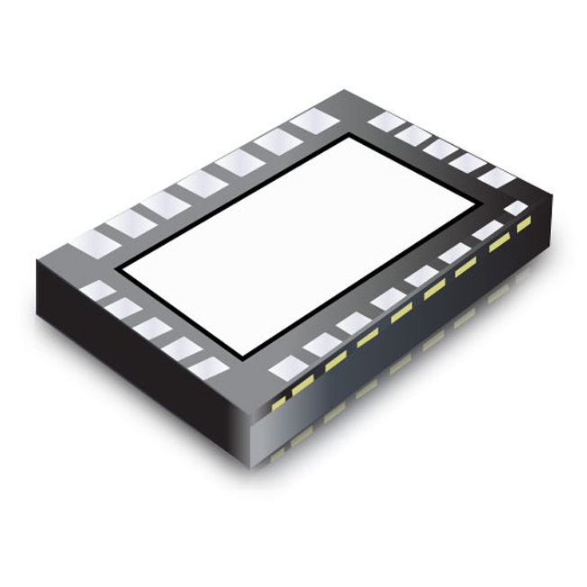
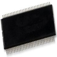
SSTV16859BS - Brand New PHILIPS Special Logic ICs
-
Description
The SSTV16859 is a 13-bit to 26-bit SSTL_2 registered driver with differential clock inputs, designed to operate between 2.3 V and 2.7 V. All inputs are compatible with the JEDEC standard for SSTL_2 with VREF normally at 0.5*VDD, except the LVCMOS reset (RESET) input. All outputs are SSTL_2, Class II compatible which can be used for standard stub-series applications or capacitive loads. Master reset (RESET) asynchronously resets all registers to zero.
The SSTV16859 is intended to be incorporated into standard DIMM (Dual In-Line Memory Module) designs defined by JEDEC, such as DDR (Double Data Rate) SDRAM and SDRAM II Memory Modules. Different from traditional SDRAM, DDR SDRAM transfers data on both clock edges (rising and falling), thus doubling the peak bus bandwidth. A DDR DRAM rated at 133 MHz will have a burst rate of 266 MHz.
The device data inputs consist of different receivers. One differential input is tied to the input pin while the other is tied to a reference input pad, which is shared by all inputs. The clock input is fully differential (CK and CK) to be compatible with DRAM devices that are installed on the DIMM. Data are registered at the crossing of CK going high, and CK going low. However, since the control inputs to the SDRAM change at only half the data rate, the device must only change state on the positive transition of the CK signal.
In order to be able to provide defined outputs from the device even before a stable clock has been supplied, the device has an asynchronous input pin (RESET), which when held to the LOW state, resets all registers and all outputs to the LOW state. The device supports low-power standby operation. When RESET is low, the differential input receivers are disabled, and undriven (floating) data, clock, and reference voltage (VREF) inputs are allowed. In addition, when RESET is low, all registers are reset, and all outputs are forced low.
To ensure defined outputs from the register before a stable clock has been supplied, RESET must be held in the low state during power-up. In the DDR DIMM application, RESET is specified to be completely asynchronous with respect to CK and CK. Therefore, no timing relationship can be guaranteed between the two. When entering RESET, the register will be cleared and the outputs will be driven low. As long as the data inputs are low, and the clock is stable during the time from the low-to-high transition of RESET until the input receivers are fully enabled, the outputs will remain low. Available in 64-pin plastic thin shrink small outline package.
Specifications and features
• Stub-series terminated logic for 2.5 V VDD (SSTL_2)
• Optimized for stacked DDR (Double Data Rate) SDRAM applications
• Supports SSTL_2 signal inputs as per JESD 8–9
• Flow-through architecture optimizes PCB layout
• ESD classification testing is done to JEDEC Standard JESD22. Protection exceeds 2000 V to HBM per method A114.
• Latch-up testing is done to JEDEC Standard JESD78, which exceeds 100 mA.
• Supports efficient low power standby operation
• Full DDR 200/266 solution for stacked DIMMs at 2.5 V when used with PCKV857
• See SSTV16857 for JEDEC compliant register support in unstacked DIMM applications
• See SSTV16856 for driver/buffer version with mode select.Application Scenarios
The SSTV16859 is designed to be incorporated into standard DIMM (Dual In-Line Memory Module) designs defined by JEDEC. It is suitable for use in DDR (Double Data Rate) SDRAM and SDRAM II Memory Modules. Its optimized characteristics make it ideal for stacked DDR SDRAM applications. The device supports SSTL_2 signal inputs and features a flow-through architecture that optimizes PCB layout.
Comparison
Advantages- Stub-series terminated logic for 2.5 V VDD (SSTL_2)
- Optimized for stacked DDR SDRAM applications
- Efficient low-power standby operationDisadvantages- No timing relationship can be guaranteed between RESET and CK/CK signals
- LVCMOS RESET input must always be held at a valid logic high or low level. -
Similar parts: 578 , Click to view
-
Datasheet
-
Shopping guide
Delivery period:
- - Will ship out in 2-3 days
- - DHL Express: 3-7 business days
- - DHL eCommerce: 12-22 business days
- - FedEx International Priority: 3-7 business days
- - EMS: 10-15 business days
Shipping fee:
- - Automatic Email notification (above 5 times)
- - View in your order page
Shipping option:
DHL, FedEx, EMS, SF Express, and Registered Air MailShipping tracking:
- - Automatic Email notification (above 5 times)
- - View in your order page
How to Buy:
- - In-stock, Add to cart > Check out > Submit order > Complete payment >Delivery.
- - Inquiry, Add to inquiry sheet/Submit bom/inquire file/Send email us > Quote > Place order > Complete payment >Delivery.
- View more
Payment:
- - Paypal,Credit Card includes Visa, Master, American Express.
- - Wire transfer, include Local bank transfer.
- - Western Union.
- View more
- Datasheet: Download SSTV16859BS
- Chipdatas Part: CD87-SSTV16859BS
- Warehouse: China, Hong Kong
- Dispatch: Within 24 hours
- Free Shipping: Yes
- Prority Shipping: Yes, 3-5 days
- Last Updated: 2024/10/01 16:47 +0800
-
- Full Refund if you don't receive your order
- Full or Partial Refund , If the item is not as described
-
 PI74SSTV16857A - Brand New Diodes Incorporated Special Logic ICsTSSOP-48
 -
 MC10EL16D - Brand New ON Semiconductor Special Logic ICsSOIC-8
 -
 DM74LS83AN - Brand New onsemi Special Logic ICs16-DIP 0.300", 7.62mm
 -
 MC14007UB - Brand New MOTOROLA Special Logic ICsDIP-14
 -
 LM9780CCVS - Brand New Texas Instruments Special Logic ICsQFP
 -
 74LVTH182512DGGR - Brand New Texas Instruments Special Logic ICsTSSOP-64
 -
 74ABT899C - Brand New onsemi Special Logic ICsSOP-28
 -
 74F656AD - Brand New PHILIPS Special Logic ICsSOP7.2MM
 -
 74SSTV16859PA - Brand New IDT Special Logic ICsTSSOP-64
 -
 32864AH - Brand New Littelfuse Special Logic ICsBGA
-
The fee is charged according to the rule of PayPal.
-
The fee is charged according to the rule of PayPal.
-
Western Union charge US$0.00 banking fee.
-
We recommend to use bank transfer for large orders to save on handling fees.
-
DHL(www.dhl.com)
$40 limited time offer. -
UPS(www.ups.com)
$40 limited time offer. -
FedEx(www.fedex.com)
$40 limited time offer. -
Registered Mail(www.singpost.com)
Free shipping without minimum order.
