ADN2812ACPZ-RL7 - Brand New Analog Devices Clock / Timing - Application Specific
In Stock:2931 ,Ready for Immediate Shipping
New
RoSH Lead free
In Stock:
2931,
Ready for Immediate Shipping
Brand:Analog Devices
Chipdatas Part No.:CD86-ADN2812ACPZ-RL7
Manufacturer Part No.:ADN2812ACPZ-RL7
Datecode:09+
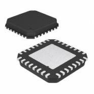
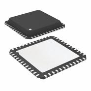
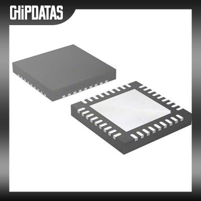
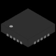
Package:32-VFQFN Exposed Pad, CSP
88,35700 US$ /PCS
Each contains 0 PCS
≥1:
88,35700 US$
≥10:
87,47343 US$
≥50:
86,58986 US$
≥100:
83,93915 US$
-
Description
The ADN2812ACPZ-RL7 is an electronic component that belongs to the clock/timing - application specific product category. It offers receiver functions of quantization, signal level detect, and clock and data recovery for continuous data rates ranging from 12.3 Mb/s to 2.7 Gb/s. With an automatic lock feature, the ADN2812 can lock to all data rates without the need for external reference clocks or programming. All SONET jitter requirements are met, including jitter transfer, jitter generation, and jitter tolerance. The ADN2812 is designed to work under temperatures ranging from -40℃ to +85℃.
Specifications and features
- Serial data input: 12.3 Mb/s to 2.7 Gb/s
- Quantizer sensitivity: 6 mV typical
- Adjustable slice level: ±100 mV
- Patented clock recovery architecture
- Loss of signal (LOS) detect range: 3 mV to 15 mV
- Independent slice level adjust and LOS detector
- No reference clock required
- Loss of lock indicator
- I2C interface to access optional features
- Single-supply operation: 3.3 V
- Low power: 750 mW typical
- 5 mm × 5 mm 32-lead LFCSP
Application Scenarios
The ADN2812 is suitable for a range of applications, including:
- SONET OC-1/OC-3/OC-12/OC-48 and all associated FEC rates
- Fibre Channel, 2× Fibre Channel, GbE, HDTV
- WDM transponders
- Regenerators/repeaters
- Test equipment
- Broadband cross-connects and routers
Comparison
Advantages- The ADN2812 can automatically lock to all data rates without the need for external reference clocks or programming.
- It meets all SONET jitter requirements, including jitter transfer, jitter generation, and jitter tolerance.
- The ADN2812 has an independent slice level adjust and LOS detector, allowing for greater operational control.
- It is designed to work under temperatures ranging from -40℃ to +85℃.
- With a low power consumption of 750mW typical, it is a power-efficient option.
Disadvantages- The ADN2812 has a limited application range, specific to the clock/timing - application specific product category.
-
Similar parts: 1594 , Click to view
-
Datasheet
-
Shopping guide
Delivery period:
- - Will ship out in 2-3 days
- - DHL Express: 3-7 business days
- - DHL eCommerce: 12-22 business days
- - FedEx International Priority: 3-7 business days
- - EMS: 10-15 business days
Shipping fee:
- - Automatic Email notification (above 5 times)
- - View in your order page
Shipping option:
DHL, FedEx, EMS, SF Express, and Registered Air MailShipping tracking:
- - Automatic Email notification (above 5 times)
- - View in your order page
How to Buy:
- - In-stock, Add to cart > Check out > Submit order > Complete payment >Delivery.
- - Inquiry, Add to inquiry sheet/Submit bom/inquire file/Send email us > Quote > Place order > Complete payment >Delivery.
- View more
Payment:
- - Paypal,Credit Card includes Visa, Master, American Express.
- - Wire transfer, include Local bank transfer.
- - Western Union.
- View more
-
Popular parts of the same kind
Additional Information
- Datasheet: Download ADN2812ACPZ-RL7
- Chipdatas Part: CD86-ADN2812ACPZ-RL7
- Warehouse: China, Hong Kong
- Dispatch: Within 24 hours
- Free Shipping: Yes
- Prority Shipping: Yes, 3-5 days
- Last Updated: 2024/05/20 12:28 +0800
Refund
-
- Full Refund if you don't receive your order
- Full or Partial Refund , If the item is not as described
Related Products
-
 ADN2855ACPZ - Brand New Analog Devices Clock / Timing - Application Specific32-VFQFN Exposed Pad, CSP
 -
 AD9524BCPZ - Brand New Analog Devices Clock / Timing - Application SpecificLFCSP
 -
 AD9524BCPZ - Brand New ADI Clock / Timing - Application SpecificLFCSP-48-VQ7x7
 -
 SI5324D-C-GM - Brand New SILICON LABS Clock / Timing - Application SpecificQFN-36-EP6x6
 -
ADN2855ACPZ - Brand New ADI Clock / Timing - Application SpecificLFCSP-32-VQ5x5
-
 EL5001ILZ - Brand New RENESAS Clock / Timing - Application SpecificQFN-20
 -
 CV115-4PVG - Brand New IDT Clock / Timing - Application SpecificSSOP
 -
 CV146PVG - Brand New IDT Clock / Timing - Application SpecificSSOP-56
 -
 CSPU877 - Brand New IDT Clock / Timing - Application SpecificBGA
 -
 ZL30122 - Brand New Zarlink Clock / Timing - Application SpecificBGA
Payment Method
-
The fee is charged according to the rule of PayPal.
-
The fee is charged according to the rule of PayPal.
-
Western Union charge US$0.00 banking fee.
-
We recommend to use bank transfer for large orders to save on handling fees.
Shipping Tips
-
DHL(www.dhl.com)
$40 limited time offer. -
UPS(www.ups.com)
$40 limited time offer. -
FedEx(www.fedex.com)
$40 limited time offer. -
Registered Mail(www.singpost.com)
Free shipping without minimum order.
