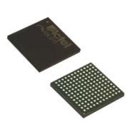
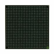
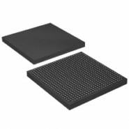
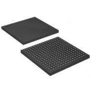
A3P400-FGG144I - Brand New Microchip Technology FPGAs (Field Programmable Gate Array)
-
Description
A3P400-FGG144I is a model of electronic component belonging to the category of FPGAs (Field Programmable Gate Array). It is part of the ProASIC3 family of Actel flash FPGAs, which offers superior performance, density, and features compared to the ProASICPLUS® family. With its nonvolatile flash technology, the ProASIC3 devices provide a secure, low-power, single-chip solution that is live at power-up (LAPU). They are reprogrammable and offer time-to-market benefits at an ASIC-level unit cost, allowing designers to create high-density systems using existing ASIC or FPGA design flows and tools.
Specifications and features
- High Capacity: 15 k to 1 M System Gates, Up to 144 kbits of True Dual-Port SRAM, Up to 300 User I/Os
- Reprogrammable Flash Technology: 130-nm, 7-Layer Metal (6 Copper), Flash-Based CMOS Process, Live at Power-Up (LAPU) Level 0 Support, Single-Chip Solution, Retains Programmed Design when Powered Off
- High Performance: 350 MHz System Performance, 3.3 V, 66 MHz 64-Bit PCI†
- In-System Programming (ISP) and Security: Secure ISP Using On-Chip 128-Bit Advanced Encryption Standard (AES) Decryption (except ARM-enabled ProASIC®3 devices) via JTAG (IEEE 1532–compliant)†, FlashLock® to Secure FPGA Contents
- Low Power: Core Voltage for Low Power, Support for 1.5 V-Only Systems, Low-Impedance Flash Switches
- High-Performance Routing Hierarchy: Segmented, Hierarchical Routing and Clock Structure
- Advanced I/O: 700 Mbps DDR, LVDS-Capable I/Os (A3P250 and above), Mixed-Voltage Operation (1.5 V, 1.8 V, 2.5 V, and 3.3 V), Bank-Selectable I/O Voltages (up to 4 Banks per Chip), Various Single-Ended and Differential I/O Standards, I/O Registers on Input, Output, and Enable Paths, Hot-Swappable and Cold Sparing I/Os‡, Programmable Output Slew Rate† and Drive Strength, Weak Pull-Up/-Down, IEEE 1149.1 (JTAG) Boundary Scan Test, Pin-Compatible Packages across the ProASIC3 Family
- Clock Conditioning Circuit (CCC) and PLL†: Six CCC Blocks, One with an Integrated PLL, Configurable Phase-Shift, Multiply/Divide, Delay Capabilities and External Feedback, Wide Input Frequency Range (1.5 MHz to 350 MHz)
- Embedded Memory†: 1 kbit of FlashROM User Nonvolatile Memory, SRAMs and FIFOs with Variable-Aspect-Ratio 4,608-Bit RAM Blocks (×1, ×2, ×4, ×9, and ×18 organizations)†, True Dual-Port SRAM (except ×18)
- ARM Processor Support in ProASIC3 FPGAs: M1 and M7 ProASIC3 Devices—Cortex-M1 and CoreMP7 Soft Processor Available with or without Debug
Application Scenarios
The A3P400-FGG144I electronic component is suitable for a wide range of application scenarios. It can be used in high-density systems, leveraging existing ASIC or FPGA design flows and tools. Its reprogrammable nature and time-to-market benefits make it ideal for designing complex electronics. Additionally, its low power consumption and secure flash technology make it a reliable choice for various industries.
Comparison
Advantages- Superior performance, density, and features compared to previous generations
- Secure, low-power, single-chip solution with live at power-up capability
- Reprogrammable and offers time-to-market benefits at an ASIC-level unit cost
- High capacity with ample system gates, dual-port SRAM, and user I/Os
- Supports various I/O standards and voltages for flexibility
- Advanced features such as in-system programming, security encryption, and clock conditioning circuit
Disadvantages- Not suitable for applications requiring very low power consumption
- Limited availability of ARM processor support for certain devices
-
Similar parts: 3140 , Click to view
-
Datasheet
-
Shopping guide
Delivery period:
- - Will ship out in 2-3 days
- - DHL Express: 3-7 business days
- - DHL eCommerce: 12-22 business days
- - FedEx International Priority: 3-7 business days
- - EMS: 10-15 business days
Shipping fee:
- - Automatic Email notification (above 5 times)
- - View in your order page
Shipping option:
DHL, FedEx, EMS, SF Express, and Registered Air MailShipping tracking:
- - Automatic Email notification (above 5 times)
- - View in your order page
How to Buy:
- - In-stock, Add to cart > Check out > Submit order > Complete payment >Delivery.
- - Inquiry, Add to inquiry sheet/Submit bom/inquire file/Send email us > Quote > Place order > Complete payment >Delivery.
- View more
Payment:
- - Paypal,Credit Card includes Visa, Master, American Express.
- - Wire transfer, include Local bank transfer.
- - Western Union.
- View more
- Datasheet: Download A3P400-FGG144I
- Chipdatas Part: CD93-A3P400-FGG144I
- Warehouse: China, Hong Kong
- Dispatch: Within 24 hours
- Free Shipping: Yes
- Prority Shipping: Yes, 3-5 days
- Last Updated: 2024/06/13 08:14 +0800
-
- Full Refund if you don't receive your order
- Full or Partial Refund , If the item is not as described
-
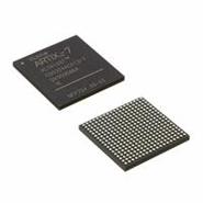 XC6SLX45-3CSG324I - Brand New XILINX FPGAs (Field Programmable Gate Array)CSBGA-324
 -
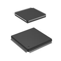 APA075-PQG208 - Brand New Microchip Technology FPGAs (Field Programmable Gate Array)208-BFQFP
 -
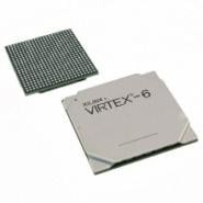 XC6VLX130T-1FFG784C - Brand New XILINX FPGAs (Field Programmable Gate Array)784-BBGA, FCBGA
 -
 XC4VFX20-11FFG672I - Brand New XILINX FPGAs (Field Programmable Gate Array)672-BBGA, FCBGA
 -
 EP2S60F672I4N - Brand New Intel / Altera FPGAs (Field Programmable Gate Array)672-BBGA, FCBGA
 -
 XC4VFX100-10FFG1517C - Brand New XILINX FPGAs (Field Programmable Gate Array)1517-BBGA, FCBGA
 -
 EP3C40F484C6N - Brand New Intel / Altera FPGAs (Field Programmable Gate Array)484-BGA
 -
 LFXP3C-3TN144C - Brand New Lattice Semiconductor FPGAs (Field Programmable Gate Array)144-LQFP
 -
 XCV50-4FG256C - Brand New XILINX FPGAs (Field Programmable Gate Array)256-BGA
 -
 EP4CE30F23C8N - Brand New Intel / Altera FPGAs (Field Programmable Gate Array)BGA
-
The fee is charged according to the rule of PayPal.
-
The fee is charged according to the rule of PayPal.
-
Western Union charge US$0.00 banking fee.
-
We recommend to use bank transfer for large orders to save on handling fees.
-
DHL(www.dhl.com)
$40 limited time offer. -
UPS(www.ups.com)
$40 limited time offer. -
FedEx(www.fedex.com)
$40 limited time offer. -
Registered Mail(www.singpost.com)
Free shipping without minimum order.
