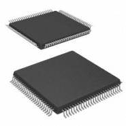
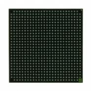
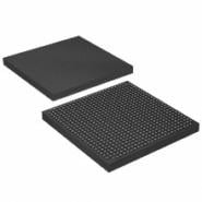
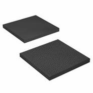
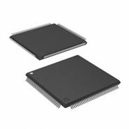
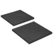
A3P030-VQ100I - Brand New Microchip Technology FPGAs (Field Programmable Gate Array)
-
Features and Benefits
High Capacity
• 15 k to 1 M System Gates
• Up to 144 kbits of True Dual-Port SRAM
• Up to 300 User I/Os
Reprogrammable Flash Technology
• 130-nm, 7-Layer Metal (6 Copper), Flash-Based CMOS Process
• Instant On Level 0 Support
• Single-Chip Solution
• Retains Programmed Design when Powered Off
High Performance
• 350 MHz System Performance
• 3.3 V, 66 MHz 64-Bit PCI†
In-System Programming (ISP) and Security
• ISP Using On-Chip 128-Bit Advanced Encryption Standard (AES) Decryption (except ARM®-enabled ProASIC®3 devices) via JTAG (IEEE 1532–compliant)†
• FlashLock® to Secure FPGA Contents
Low Power
• Core Voltage for Low Power
• Support for 1.5 V-Only Systems
• Low-Impedance Flash Switches
High-Performance Routing Hierarchy
• Segmented, Hierarchical Routing and Clock Structure
Advanced I/O
• 700 Mbps DDR, LVDS-Capable I/Os (A3P250 and above)
• 1.5 V, 1.8 V, 2.5 V, and 3.3 V Mixed-Voltage Operation
• Wide Range Power Supply Voltage Support per JESD8-B, Allowing I/Os to Operate from 2.7 V to 3.6 V
• Bank-Selectable I/O Voltages—up to 4 Banks per Chip
• Single-Ended I/O Standards: LVTTL, LVCMOS 3.3 V / 2.5 V / 1.8 V / 1.5 V, 3.3 V PCI / 3.3 V PCI-X† and LVCMOS 2.5 V / 5.0 V Input
• Differential I/O Standards: LVPECL, LVDS, B-LVDS, and M-LVDS (A3P250 and above)
• I/O Registers on Input, Output, and Enable Paths
• Hot-Swappable and Cold Sparing I/Os‡
• Programmable Output Slew Rate† and Drive Strength
• Weak Pull-Up/-Down
• IEEE 1149.1 (JTAG) Boundary Scan Test
• Pin-Compatible Packages across the ProASIC3 Family
Clock Conditioning Circuit (CCC) and PLL†
• Six CCC Blocks, One with an Integrated PLL
• Configurable Phase-Shift, Multiply/Divide, Delay Capabilities and External Feedback
• Wide Input Frequency Range (1.5 MHz to 350 MHz)
Embedded Memory†
• 1 kbit of FlashROM User Nonvolatile Memory
• SRAMs and FIFOs with Variable-Aspect-Ratio 4,608-Bit RAM Blocks (×1, ×2, ×4, ×9, and ×18 organizations)†
• True Dual-Port SRAM (except ×18)
ARM Processor Support in ProASIC3 FPGAs
• M1 ProASIC3 Devices—ARM®Cortex™-M1 Soft Processor Available with or without Debug -
Similar parts: 3140 , Click to view
-
Datasheet
-
Shopping guide
Delivery period:
- - Will ship out in 2-3 days
- - DHL Express: 3-7 business days
- - DHL eCommerce: 12-22 business days
- - FedEx International Priority: 3-7 business days
- - EMS: 10-15 business days
Shipping fee:
- - Automatic Email notification (above 5 times)
- - View in your order page
Shipping option:
DHL, FedEx, EMS, SF Express, and Registered Air MailShipping tracking:
- - Automatic Email notification (above 5 times)
- - View in your order page
How to Buy:
- - In-stock, Add to cart > Check out > Submit order > Complete payment >Delivery.
- - Inquiry, Add to inquiry sheet/Submit bom/inquire file/Send email us > Quote > Place order > Complete payment >Delivery.
- View more
Payment:
- - Paypal,Credit Card includes Visa, Master, American Express.
- - Wire transfer, include Local bank transfer.
- - Western Union.
- View more
- Datasheet: Download A3P030-VQ100I
- Chipdatas Part: CD93-A3P030-VQ100I
- Warehouse: China, Hong Kong
- Dispatch: Within 24 hours
- Free Shipping: Yes
- Prority Shipping: Yes, 3-5 days
- Last Updated: 2024/06/03 12:08 +0800
-
- Full Refund if you don't receive your order
- Full or Partial Refund , If the item is not as described
-
 XC6SLX45-3CSG324I - Brand New XILINX FPGAs (Field Programmable Gate Array)CSBGA-324
 -
 APA075-PQG208 - Brand New Microchip Technology FPGAs (Field Programmable Gate Array)208-BFQFP
 -
 XC6VLX130T-1FFG784C - Brand New XILINX FPGAs (Field Programmable Gate Array)784-BBGA, FCBGA
 -
 XC4VFX20-11FFG672I - Brand New XILINX FPGAs (Field Programmable Gate Array)672-BBGA, FCBGA
 -
 EP2S60F672I4N - Brand New Intel / Altera FPGAs (Field Programmable Gate Array)672-BBGA, FCBGA
 -
 XC4VFX100-10FFG1517C - Brand New XILINX FPGAs (Field Programmable Gate Array)1517-BBGA, FCBGA
 -
 EP3C40F484C6N - Brand New Intel / Altera FPGAs (Field Programmable Gate Array)484-BGA
 -
 LFXP3C-3TN144C - Brand New Lattice Semiconductor FPGAs (Field Programmable Gate Array)144-LQFP
 -
 XCV50-4FG256C - Brand New XILINX FPGAs (Field Programmable Gate Array)256-BGA
 -
 EP4CE30F23C8N - Brand New Intel / Altera FPGAs (Field Programmable Gate Array)BGA
-
The fee is charged according to the rule of PayPal.
-
The fee is charged according to the rule of PayPal.
-
Western Union charge US$0.00 banking fee.
-
We recommend to use bank transfer for large orders to save on handling fees.
-
DHL(www.dhl.com)
$40 limited time offer. -
UPS(www.ups.com)
$40 limited time offer. -
FedEx(www.fedex.com)
$40 limited time offer. -
Registered Mail(www.singpost.com)
Free shipping without minimum order.
