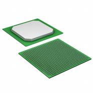
EP2C50F672C6N - Brand New Intel / Altera FPGAs (Field Programmable Gate Array)
-
Description
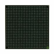
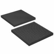
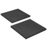
The EP2C50F672C6N is an electronic component model from the FPGAs category. It is part of the second-generation Cyclone II device family developed by Altera. This model offers a high-density architecture, with a range of 4,608 to 68,416 logic elements (LEs). It also provides up to 622 usable I/O pins and up to 1.1 Mbits of embedded memory. The Cyclone II FPGAs are manufactured using TSMCs 90-nm low-k dielectric process, ensuring both rapid availability and low cost.
Specifications and features
- High-density architecture with 4,608 to 68,416 LEs
- M4K embedded memory blocks
- Up to 1.1 Mbits of RAM available without reducing available logic
- 4,096 memory bits per block (4,608 bits per block including 512 parity bits)
- Variable port configurations of ×1, ×2, ×4, ×8, ×9, ×16, ×18, ×32, and ×36
- True dual-port operation for ×1, ×2, ×4, ×8, ×9, ×16, and ×18 modes
- Byte enables for data input masking during writes
- Up to 260-MHz operation
- Embedded multipliers with up to 150 18- × 18-bit multipliers configurable as two independent 9- × 9-bit multipliers with up to 250-MHz performance
- Optional input and output registers
- Advanced I/O support with various high-speed differential and single-ended I/O standards
- Peripheral Component Interconnect Special Interest Group (PCI SIG) PCI Local Bus Specification, Revision 3.0 compliance
- PCI Express support
- High-speed external memory support, including DDR, DDR2, and SDR SDRAM, and QDRII SRAM
- Dedicated registers per I/O element (IOE)
- Programmable bus-hold feature
- Programmable output drive strength feature
- Programmable delays from the pin to the IOE or logic array
- I/O bank grouping for unique VCCIO and/or VREF bank settings
- MultiVolt™ I/O standard support
- Hot-socketing operation support
- Tri-state with weak pull-up on I/O pins before and during configuration
- Programmable open-drain outputs
- Series on-chip termination supportApplication Scenarios
This electronic component model is suitable for various applications that require high-density programmable logic. Its features, such as the embedded memory, multipliers, advanced I/O support, and high-speed external memory compatibility, make it ideal for use in industries such as telecommunications, automotive, robotics, and aerospace. It can be used in the development of communication systems, signal processing applications, control systems, and data storage solutions.
Comparison
Advantages- High-density architecture provides a wide range of logic elements and embedded memory, offering versatility for different application requirements.
- The FPGA's compatibility with various high-speed differential and single-ended I/O standards enables seamless integration with other components.
- The support for multiple port configurations and true dual-port operation enhances flexibility and data processing capabilities.
- The programmable features, such as output drive strength, bus-hold, and delays, allow for customization and optimization of performance.
Disadvantages- The advanced features and high-density architecture may require a steep learning curve and extensive expertise in FPGA programming and integration.
- The compatibility with different memory types and I/O standards might require additional external components or adapters for specific applications.
- The extensive range of features and specifications may incur a higher cost compared to other FPGA models with more basic functionalities.
-
Similar parts: 3140 , Click to view
-
Datasheet
-
Shopping guide
Delivery period:
- - Will ship out in 2-3 days
- - DHL Express: 3-7 business days
- - DHL eCommerce: 12-22 business days
- - FedEx International Priority: 3-7 business days
- - EMS: 10-15 business days
Shipping fee:
- - Automatic Email notification (above 5 times)
- - View in your order page
Shipping option:
DHL, FedEx, EMS, SF Express, and Registered Air MailShipping tracking:
- - Automatic Email notification (above 5 times)
- - View in your order page
How to Buy:
- - In-stock, Add to cart > Check out > Submit order > Complete payment >Delivery.
- - Inquiry, Add to inquiry sheet/Submit bom/inquire file/Send email us > Quote > Place order > Complete payment >Delivery.
- View more
Payment:
- - Paypal,Credit Card includes Visa, Master, American Express.
- - Wire transfer, include Local bank transfer.
- - Western Union.
- View more
- Datasheet: Download EP2C50F672C6N
- Chipdatas Part: CD94-EP2C50F672C6N
- Warehouse: China, Hong Kong
- Dispatch: Within 24 hours
- Free Shipping: Yes
- Prority Shipping: Yes, 3-5 days
- Last Updated: 2024/06/13 02:49 +0800
-
- Full Refund if you don't receive your order
- Full or Partial Refund , If the item is not as described
-
 XC6SLX45-3CSG324I - Brand New XILINX FPGAs (Field Programmable Gate Array)CSBGA-324
 -
 APA075-PQG208 - Brand New Microchip Technology FPGAs (Field Programmable Gate Array)208-BFQFP
 -
 XC6VLX130T-1FFG784C - Brand New XILINX FPGAs (Field Programmable Gate Array)784-BBGA, FCBGA
 -
 XC4VFX20-11FFG672I - Brand New XILINX FPGAs (Field Programmable Gate Array)672-BBGA, FCBGA
 -
 EP2S60F672I4N - Brand New Intel / Altera FPGAs (Field Programmable Gate Array)672-BBGA, FCBGA
 -
 XC4VFX100-10FFG1517C - Brand New XILINX FPGAs (Field Programmable Gate Array)1517-BBGA, FCBGA
 -
 EP3C40F484C6N - Brand New Intel / Altera FPGAs (Field Programmable Gate Array)484-BGA
 -
 LFXP3C-3TN144C - Brand New Lattice Semiconductor FPGAs (Field Programmable Gate Array)144-LQFP
 -
 XCV50-4FG256C - Brand New XILINX FPGAs (Field Programmable Gate Array)256-BGA
 -
 EP4CE30F23C8N - Brand New Intel / Altera FPGAs (Field Programmable Gate Array)BGA
-
The fee is charged according to the rule of PayPal.
-
The fee is charged according to the rule of PayPal.
-
Western Union charge US$0.00 banking fee.
-
We recommend to use bank transfer for large orders to save on handling fees.
-
DHL(www.dhl.com)
$40 limited time offer. -
UPS(www.ups.com)
$40 limited time offer. -
FedEx(www.fedex.com)
$40 limited time offer. -
Registered Mail(www.singpost.com)
Free shipping without minimum order.
