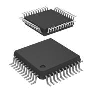
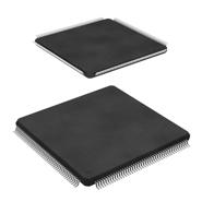
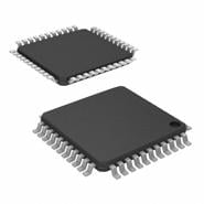
ST72F324BJ6TA - Brand New STMicroelectronics Microcontrollers
-
INTRODUCTION
The ST72324K and ST72324J devices are members of the ST7 microcontroller family. They can be grouped as follows:
– The 32-pin ST72324K devices are designed for mid-range applications
– The 42/44-pin ST72324J devices target the same range of applications requiring more than 24 I/O ports.All devices are based on a common industrystandard 8-bit core, featuring an enhanced instruction set and are available with FLASH or ROM program memory.
■ Memories
– 8 to 32K dual voltage High Density Flash (HDFlash) or ROM with read-out protection capability. In-Application Programming and InCircuit Programming for HDFlash devices
– 384 to 1K bytes RAM
– HDFlash endurance: 100 cycles, data retention: 20 years at 55°C
■ Clock, Reset And Supply Management
– Enhanced low voltage supervisor (LVD) for main supply with 3 programmable reset thresholds and auxiliary voltage detector (AVD) with interrupt capability
– Clock sources: crystal/ceramic resonator oscillators, internal RC oscillator, clock security system and bypass for external clock
– PLL for 2x frequency multiplication
– Four Power Saving Modes: Halt, Active-Halt, Wait and Slow
■ Interrupt Management
– Nested interrupt controller
– 10 interrupt vectors plus TRAP and RESET
– 9/6 external interrupt lines (on 4 vectors)
■ Up to 32 I/O Ports
– 32/24 multifunctional bidirectional I/O lines
– 22/17 alternate function lines
– 12/10 high sink outputs
■ 4 Timers
– Main Clock Controller with: Real time base, Beep and Clock-out capabilities
– Configurable watchdog timer
– 16-bit Timer A with: 1 input capture, 1 output compare, external clock input, PWM and pulse generator modes
– 16-bit Timer B with: 2 input captures, 2 output compares, PWM and pulse generator modes
■ 2 Communication Interfaces
– SPI synchronous serial interface
– SCI asynchronous serial interface (LIN compatible)
■ 1 Analog Peripheral
– 10-bit ADC with up to 12 input pins
■ Instruction Set
– 8-bit Data Manipulation
– 63 Basic Instructions
– 17 main Addressing Modes
– 8 x 8 Unsigned Multiply Instruction
■ Development Tools
– Full hardware/software development package
– In-Circuit Testing capability -
Similar parts: 10206 , Click to view
-
Datasheet
-
Shopping guide
Delivery period:
- - Will ship out in 2-3 days
- - DHL Express: 3-7 business days
- - DHL eCommerce: 12-22 business days
- - FedEx International Priority: 3-7 business days
- - EMS: 10-15 business days
Shipping fee:
- - Automatic Email notification (above 5 times)
- - View in your order page
Shipping option:
DHL, FedEx, EMS, SF Express, and Registered Air MailShipping tracking:
- - Automatic Email notification (above 5 times)
- - View in your order page
How to Buy:
- - In-stock, Add to cart > Check out > Submit order > Complete payment >Delivery.
- - Inquiry, Add to inquiry sheet/Submit bom/inquire file/Send email us > Quote > Place order > Complete payment >Delivery.
- View more
Payment:
- - Paypal,Credit Card includes Visa, Master, American Express.
- - Wire transfer, include Local bank transfer.
- - Western Union.
- View more
-
Popular parts of the same kind
- Datasheet: Download ST72F324BJ6TA
- Chipdatas Part: CD93-ST72F324BJ6TA
- Warehouse: China, Hong Kong
- Dispatch: Within 24 hours
- Free Shipping: Yes
- Prority Shipping: Yes, 3-5 days
- Last Updated: 2024/10/02 11:43 +0800
-
- Full Refund if you don't receive your order
- Full or Partial Refund , If the item is not as described
-
 PIC12F675T-I/SN - Brand New Microchip Technology Microcontrollers8-SOIC 0.154", 3.90mm Width
 -
 PIC18F252-I/SO - Brand New Microchip Technology Microcontrollers28-SOIC 0.295", 7.50mm Width
 -
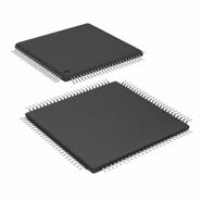 PIC32MX775F256L-80I/PT - Brand New Microchip Technology Microcontrollers100-TQFP
 -
 PIC32MX695F512H-80I/PT - Brand New Microchip Technology MicrocontrollersTQFP-64
 -
 STM32F205RBT6 - Brand New STMicroelectronics MicrocontrollersLQFP-64
 -
 STM8S003F3P6TR - Brand New STMicroelectronics MicrocontrollersTSSOP-20
 -
 PIC18F8621-I/PT - Brand New Microchip Technology MicrocontrollersQFP
 -
 STM32F103R8T6 - Brand New STMicroelectronics MicrocontrollersLQFP-64
 -
 STM32F429IGT6 - Brand New STMicroelectronics MicrocontrollersLQFP-176
 -
 DSPIC33FJ128GP804-I/PT - Brand New Microchip Technology Microcontrollers44-TQFP
-
The fee is charged according to the rule of PayPal.
-
The fee is charged according to the rule of PayPal.
-
Western Union charge US$0.00 banking fee.
-
We recommend to use bank transfer for large orders to save on handling fees.
-
DHL(www.dhl.com)
$40 limited time offer. -
UPS(www.ups.com)
$40 limited time offer. -
FedEx(www.fedex.com)
$40 limited time offer. -
Registered Mail(www.singpost.com)
Free shipping without minimum order.
