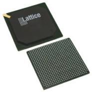
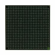
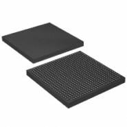
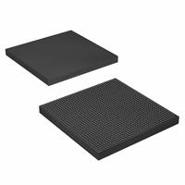
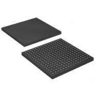
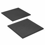
LFE3-70EA-7FN672I - Brand New LATTICE FPGAs (Field Programmable Gate Array)
-
Description
The LFE3-70EA-7FN672I is a model of FPGA (Field Programmable Gate Array) in the LatticeECP3™ family. It is designed to deliver high performance features with an enhanced DSP architecture, high speed SERDES, and high speed source synchronous interfaces. The device is made using 65 nm technology, which makes it suitable for high-volume, high-speed, low-cost applications.
Specifications and features
- Logic Density: 17K to 149K LUTs
- I/Os: 116 to 586
- Embedded SERDES: Supports generic 8b10b, 10-bit SERDES, and 8-bit SERDES modes with data rates from 150 Mbps to 3.2 Gbps per channel for various protocols such as PCI Express, SONET/SDH, Ethernet, CPRI, SMPTE 3G, and Serial RapidIO
- sysDSP™: Cascadable slice architecture with 12 to 160 slices for high performance multiply and accumulate operations
- Flexible Memory Resources: Up to 6.85Mbits sysMEM™ Embedded Block RAM (EBR) and 36K to 303K bits distributed RAM
- sysCLOCK Analog PLLs and DLLs: Two DLLs and up to ten PLLs per device
- Pre-Engineered Source Synchronous I/O: Supports DDR registers, read/write leveling functionality, gearing logic, and source synchronous standards
- Programmable sysI/O™ Buffer: Supports a wide range of interfaces with on-chip termination and optional equalization filter
- Flexible Device Configuration: Includes dedicated bank for configuration I/Os, SPI boot flash interface, dual-boot images support, Slave SPI, TransFR™ I/O, and Soft Error Detect embedded macro
- System Level Support: IEEE 1149.1 and IEEE 1532 compliant, Reveal Logic Analyzer, ORCAstra FPGA configuration utility, on-chip oscillator, and 1.2 V core power supply
Application Scenarios
The LFE3-70EA-7FN672I FPGA can be used in various applications such as high-speed data processing systems, networking equipment, telecommunications devices, and embedded systems that require high performance and low cost.
Comparison
Advantages- High logic density for increased system integration
- Embedded SERDES for various protocols
- Powerful sysDSP™ for high performance multiply and accumulate operations
- Flexible memory resources for efficient data storage
- Programmable sysI/O™ Buffer for interfacing with different interfaces
- Flexible device configuration options
- System level support for easy integration
Disadvantages- Limited logic density options compared to other FPGA models
- Limited number of I/Os compared to other FPGA models
-
Similar parts: 3140 , Click to view
-
Datasheet
-
Shopping guide
Delivery period:
- - Will ship out in 2-3 days
- - DHL Express: 3-7 business days
- - DHL eCommerce: 12-22 business days
- - FedEx International Priority: 3-7 business days
- - EMS: 10-15 business days
Shipping fee:
- - Automatic Email notification (above 5 times)
- - View in your order page
Shipping option:
DHL, FedEx, EMS, SF Express, and Registered Air MailShipping tracking:
- - Automatic Email notification (above 5 times)
- - View in your order page
How to Buy:
- - In-stock, Add to cart > Check out > Submit order > Complete payment >Delivery.
- - Inquiry, Add to inquiry sheet/Submit bom/inquire file/Send email us > Quote > Place order > Complete payment >Delivery.
- View more
Payment:
- - Paypal,Credit Card includes Visa, Master, American Express.
- - Wire transfer, include Local bank transfer.
- - Western Union.
- View more
- Datasheet: Download LFE3-70EA-7FN672I
- Chipdatas Part: CD87-LFE3-70EA-7FN672I
- Warehouse: China, Hong Kong
- Dispatch: Within 24 hours
- Free Shipping: Yes
- Prority Shipping: Yes, 3-5 days
- Last Updated: 2024/06/26 09:12 +0800
-
- Full Refund if you don't receive your order
- Full or Partial Refund , If the item is not as described
-
 XC6SLX45-3CSG324I - Brand New XILINX FPGAs (Field Programmable Gate Array)CSBGA-324
 -
 APA075-PQG208 - Brand New Microchip Technology FPGAs (Field Programmable Gate Array)208-BFQFP
 -
 XC6VLX130T-1FFG784C - Brand New XILINX FPGAs (Field Programmable Gate Array)784-BBGA, FCBGA
 -
 XC4VFX20-11FFG672I - Brand New XILINX FPGAs (Field Programmable Gate Array)672-BBGA, FCBGA
 -
 EP2S60F672I4N - Brand New Intel / Altera FPGAs (Field Programmable Gate Array)672-BBGA, FCBGA
 -
 XC4VFX100-10FFG1517C - Brand New XILINX FPGAs (Field Programmable Gate Array)1517-BBGA, FCBGA
 -
 EP3C40F484C6N - Brand New Intel / Altera FPGAs (Field Programmable Gate Array)484-BGA
 -
 LFXP3C-3TN144C - Brand New Lattice Semiconductor FPGAs (Field Programmable Gate Array)144-LQFP
 -
 XCV50-4FG256C - Brand New XILINX FPGAs (Field Programmable Gate Array)256-BGA
 -
 EP4CE30F23C8N - Brand New Intel / Altera FPGAs (Field Programmable Gate Array)BGA
-
The fee is charged according to the rule of PayPal.
-
The fee is charged according to the rule of PayPal.
-
Western Union charge US$0.00 banking fee.
-
We recommend to use bank transfer for large orders to save on handling fees.
-
DHL(www.dhl.com)
$40 limited time offer. -
UPS(www.ups.com)
$40 limited time offer. -
FedEx(www.fedex.com)
$40 limited time offer. -
Registered Mail(www.singpost.com)
Free shipping without minimum order.
