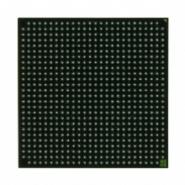
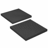
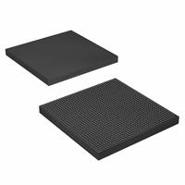
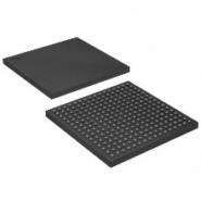
LX256V-35F484C - Brand New LATTICE FPGAs (Field Programmable Gate Array)
-
Description
The LX256V-35F484C is a model from the ispGDX2™ family, which is Lattice's second generation in-system programmable generic digital crosspoint switch for high-speed bus switching and interface applications. This family of switches combines a flexible switching architecture with advanced sysIO interfaces including high-performance sysHSI Blocks and sysCLOCK PLLs to meet the needs of today's high-speed systems. The LX256V-35F484C is available in two options: the standard device with sysHSI capability for ultra-fast serial communications, and the lower-cost "E-series" without the sysHSI block. The ispGDX2 family facilitates a variety of common switching functions through a multiplexer-intensive architecture.
Specifications and features
The LX256V-35F484C offers the following specifications and features:
- High-performance bus switching with high bandwidth up to 12.8 Gbps (SERDES) and up to 38 Gbps (without SERDES)
- Up to 16 (15x10) FIFOs for data buffering
- High-speed performance with fMAX = 360MHz, tPD = 3.0ns, tCO = 2.9ns, and tS = 2.0ns
- Built-in programmable control logic capability
- I/O intensive with 64 to 256 I/Os
- Expanded MUX capability up to 188:1 MUX
- sysCLOCK™ PLL for frequency synthesis, skew management, clock multiply and divide capability, and clock shifting
- sysIO™ Interfacing with support for various standard board interfaces
- Two options available: high-performance sysHSI version and low-cost version without sysHSI
- sysHSI Blocks provide up to 16 high-speed channels with SERDES, Clock Data Recovery (CDR), and support for various encoding techniques
- Flexible programming and testing with IEEE 1532 compliant In-System Programmability (ISP™) and boundary scan test through IEEE 1149.1 interface
- Supports various power supplies: 3.3V, 2.5V, or 1.8V
- 5V tolerant I/O for LVCMOS 3.3 and LVTTL interfaces
Application Scenarios
The LX256V-35F484C can be used in various high-speed bus switching and interface applications, such as:
- Network routers and switches
- Data storage systems
- Telecommunications equipment
- Industrial automation systems
- Test and measurement equipment
Comparison
Advantages:
- High-performance bus switching with high bandwidth
- Flexible switching architecture
- Advanced sysIO interfaces
- Multiple sysHSI Blocks for high-speed channels
- Flexible programming and testing capabilities
Disadvantages:
- The "E-series" version lacks the sysHSI capability for ultra-fast serial communications
- The LX256V-35F484C is not suitable for low-speed applications
-
Similar parts: 3140 , Click to view
-
Datasheet
-
Shopping guide
Delivery period:
- - Will ship out in 2-3 days
- - DHL Express: 3-7 business days
- - DHL eCommerce: 12-22 business days
- - FedEx International Priority: 3-7 business days
- - EMS: 10-15 business days
Shipping fee:
- - Automatic Email notification (above 5 times)
- - View in your order page
Shipping option:
DHL, FedEx, EMS, SF Express, and Registered Air MailShipping tracking:
- - Automatic Email notification (above 5 times)
- - View in your order page
How to Buy:
- - In-stock, Add to cart > Check out > Submit order > Complete payment >Delivery.
- - Inquiry, Add to inquiry sheet/Submit bom/inquire file/Send email us > Quote > Place order > Complete payment >Delivery.
- View more
Payment:
- - Paypal,Credit Card includes Visa, Master, American Express.
- - Wire transfer, include Local bank transfer.
- - Western Union.
- View more
- Datasheet: Download LX256V-35F484C
- Chipdatas Part: CD87-LX256V-35F484C
- Warehouse: China, Hong Kong
- Dispatch: Within 24 hours
- Free Shipping: Yes
- Prority Shipping: Yes, 3-5 days
- Last Updated: 2024/06/26 07:53 +0800
-
- Full Refund if you don't receive your order
- Full or Partial Refund , If the item is not as described
-
 XC6SLX45-3CSG324I - Brand New XILINX FPGAs (Field Programmable Gate Array)CSBGA-324
 -
 APA075-PQG208 - Brand New Microchip Technology FPGAs (Field Programmable Gate Array)208-BFQFP
 -
 XC6VLX130T-1FFG784C - Brand New XILINX FPGAs (Field Programmable Gate Array)784-BBGA, FCBGA
 -
 XC4VFX20-11FFG672I - Brand New XILINX FPGAs (Field Programmable Gate Array)672-BBGA, FCBGA
 -
 EP2S60F672I4N - Brand New Intel / Altera FPGAs (Field Programmable Gate Array)672-BBGA, FCBGA
 -
 XC4VFX100-10FFG1517C - Brand New XILINX FPGAs (Field Programmable Gate Array)1517-BBGA, FCBGA
 -
 EP3C40F484C6N - Brand New Intel / Altera FPGAs (Field Programmable Gate Array)484-BGA
 -
 LFXP3C-3TN144C - Brand New Lattice Semiconductor FPGAs (Field Programmable Gate Array)144-LQFP
 -
 XCV50-4FG256C - Brand New XILINX FPGAs (Field Programmable Gate Array)256-BGA
 -
 EP4CE30F23C8N - Brand New Intel / Altera FPGAs (Field Programmable Gate Array)BGA
-
The fee is charged according to the rule of PayPal.
-
The fee is charged according to the rule of PayPal.
-
Western Union charge US$0.00 banking fee.
-
We recommend to use bank transfer for large orders to save on handling fees.
-
DHL(www.dhl.com)
$40 limited time offer. -
UPS(www.ups.com)
$40 limited time offer. -
FedEx(www.fedex.com)
$40 limited time offer. -
Registered Mail(www.singpost.com)
Free shipping without minimum order.
