


 Purchase Protection
Powerful Protection from Payment to Delivery
Secure and Reliable Payment
Money Back Guarantee
Shipping and Delivery
After-Sales Service
What are IGBTs? A detailed explanation of the working principle of IGBT
In practical applications, bipolar junction transistors (BJTs) and MOSFETs are the most popular and common electronic components. However, with the continuous advancement of technology, insulated gate bipolar transistors (IGBTs) have also gradually become one of the widely used devices.
IGBT can be regarded as a fusion of BJT and MOSFET, it has the input characteristics of BJT and the output characteristics of MOSFET. Compared with BJT or MOSFET, the advantages of IGBT are that it provides larger power gain than standard bipolar junction transistors, as well as higher operating voltage and lower MOSFET input loss.
1. What are IGBTs?
IGBT is a three-terminal semiconductor device that is highly efficient and fast-switching, and its full name is Insulated Gate Bipolar Transistor.
It can be widely used in various electronic devices for efficient and fast switching, and is mainly used in amplifiers to switch and process complex waveforms through pulse width modulation (PWM).
In IGBT, the input side represents the MOS tube with gate terminal, and the output side represents the BJT with collector and emitter terminals.
Among them, the collector and emitter terminals are the conducting terminals, while the gate terminal is the control terminal for switching operation.

2. Internal structure of IGBT
The IGBT (Insulated Gate Bipolar Transistor) has three terminals, namely the collector, emitter, and gate, all of which are coated with metal layers. However, the metal material on the gate terminal also has a layer of silicon dioxide.
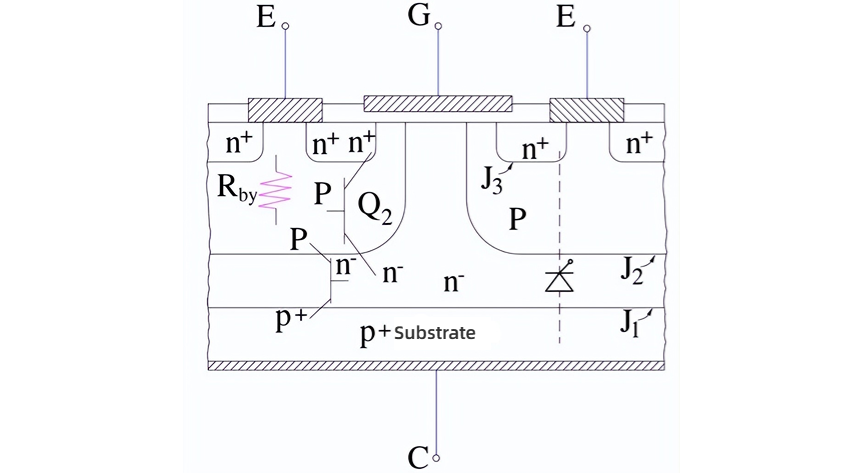
The IGBT structure is a four-layer semiconductor device. The four-layer device is achieved by combining PNP and NPN transistors, which form a PNPN arrangement.
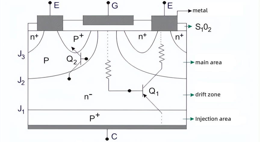
As shown in the diagram, the layer closest to the collector region is the (p+) substrate, also known as the injection region. Above it is the N-drift region, which includes an N-layer. The injection region injects most of the carrier (hole current) from (p+) into the N- layer.
The thickness of the drift region determines the IGBT's voltage blocking capability.
Above the drift region is the main region, which is composed of a (p) substrate. Near the emitter, there is an (n+) layer inside the main region.
The connection point between the injection region and the N-drift region is J2. Similarly, the connection point between the N- region and the main region is node J1.
Note: The structure of the IGBT is topologically similar to that of a "MOS" gate thyristor. However, the action and function of the thyristor can be suppressed, which means that only transistor action is allowed throughout the operating range of the IGBT device.
IGBTs are more desirable than thyristors because thyristors require fast switching at zero crossing.
3. Working principle of IGBT
IGBT is a type of semiconductor device whose operation principle is to open or close a circuit by activating or deactivating its gate terminal. When a positive input voltage passes through the gate, the emitter remains driven and the circuit remains open. Conversely, if the gate terminal voltage of the IGBT is zero or slightly negative, the circuit will be closed. IGBT can be used as both BJT and MOSFET, and the amplification achieved is the ratio between its output signal and control input signal.
For traditional BJT, the gain is roughly equal to the ratio of the output current to the input current, which we call Beta and represent as β. On the other hand, for MOSFET, there is no input current, since the gate terminal is the isolation for the main channel carrying the current. We determine the gain of IGBT by dividing the change in output current by the change in input voltage.
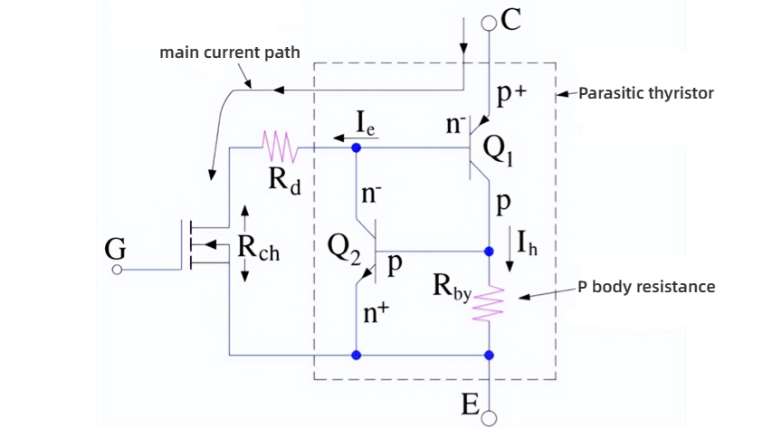
When the collector is at a positive potential relative to the emitter, the N-channel IGBT conducts, and the gate is also at a sufficiently positive potential relative to the emitter (>VGET). This causes an inversion layer to form under the gate, creating a channel, and current begins to flow from the collector to the emitter. The collector current Ic in the IGBT consists of two components, Ie and Ih. Ie is the current flowing from the collector to the emitter due to the injected electrons passing through the injection layer, drift layer, and finally forming the channel. Ih is the hole current flowing from the collector to the emitter through Q1 and the body resistance Rb. Therefore, although Ih can be almost negligible, Ic ≈ Ie.
A special phenomenon observed in IGBT is called latch-up. This occurs when the collector current exceeds a certain threshold (ICE). In this case, the parasitic thyristor is locked, and the gate terminal loses control of the collector current, and IGBT cannot be turned off even if the gate voltage drops below VGET. To turn off the IGBT, we need a typical commutation circuit, such as forced commutation with a thyristor. Failure to turn off the device promptly can result in damage to the device.
IGBT only operates when there is a voltage supply on the gate terminal, which is the gate voltage, VG. Once there is a gate voltage (VG), the gate current (IG) increases, and then it increases the gate-emitter voltage (VGE). Therefore, the gate-emitter voltage increases the collector current (IC). As a result, the collector current (IC) reduces the collector-emitter voltage (VCE). It should be noted that IGBT has a voltage drop similar to a diode, typically in the range of 2V, and only increases logarithmically with current.
IGBT uses a freewheeling diode to conduct reverse current, and the freewheeling diode is placed on the collector-emitter terminal of the IGBT.

Working principle diagram of IGBT
4. IGBT的等效电路
The approximate equivalent circuit of IGBT is composed of MOS tube and PNP transistor (Q1). Considering the resistance provided by the n-drift region, the resistance Rd is already included in the circuit, as shown in the figure below:
IGBT basic structure diagram
By carefully examining the basic structure of IGBT, we can obtain this equivalent circuit. It should be noted that the punch-through IGBT and PT-IGBT have an N+ region at the contact of the emitter. Observing the IGBT basic structure shown above, we can see that there is another path from the collector to the emitter, which includes the collector, p+, n-, p (n-channel), n+, and emitter. Therefore, there is another transistor Q2 as n-pn+ in the IGBT structure, and we need to add this transistor Q2 to the approximate equivalent circuit to obtain a more accurate equivalent circuit.
Therefore, the accurate equivalent circuit of IGBT is as follows:
IGBT accurate equivalent circuit diagram
The resistance Rby in this circuit provides a resistance for the flow of holes in the p region. As we all know, IGBT is a combination of MOS tube input and BJT output. It has a structure that is equivalent to N-channel MOS tube and Darlington-configured PNP BJT, so it can also include resistance in the drift region.
5. IGBT Characteristics--Static VI Characteristics
The figure below shows the static VI characteristics and circuit diagram with labeled parameters of an n-channel IGBT. The diagram is similar to that of a BJT, but the constant parameter maintained in the IGBT diagram is VGE. This is because IGBT is a voltage-controlled device, while BJT is a current-controlled device. When the IGBT is in the off state (VCE is positive and VGE is less than VGET), the reverse voltage is blocked by J2. When it is reverse biased, i.e. VCE is negative, J1 blocks the voltage.

6. Characteristics of IGBT--Switching Characteristics
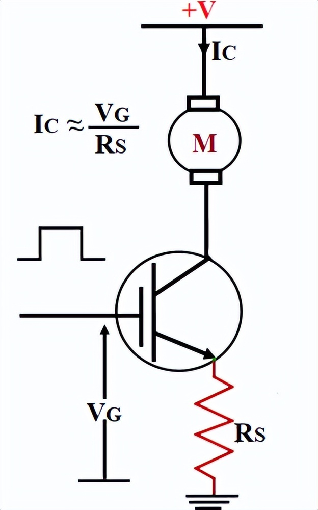
IGBT is a voltage-controlled device that only requires a small voltage at the gate to maintain its conducting state. As it is a unidirectional device, IGBT can only switch current in the forward direction from the collector to the emitter. A typical IGBT switching circuit is shown in the figure below: the gate voltage VG is applied to the gate pin, thereby switching the power supply voltage V+ of motor M. The resistor Rs is roughly used to limit the current through the motor.
The figure below shows the typical switching characteristics of IGBT.
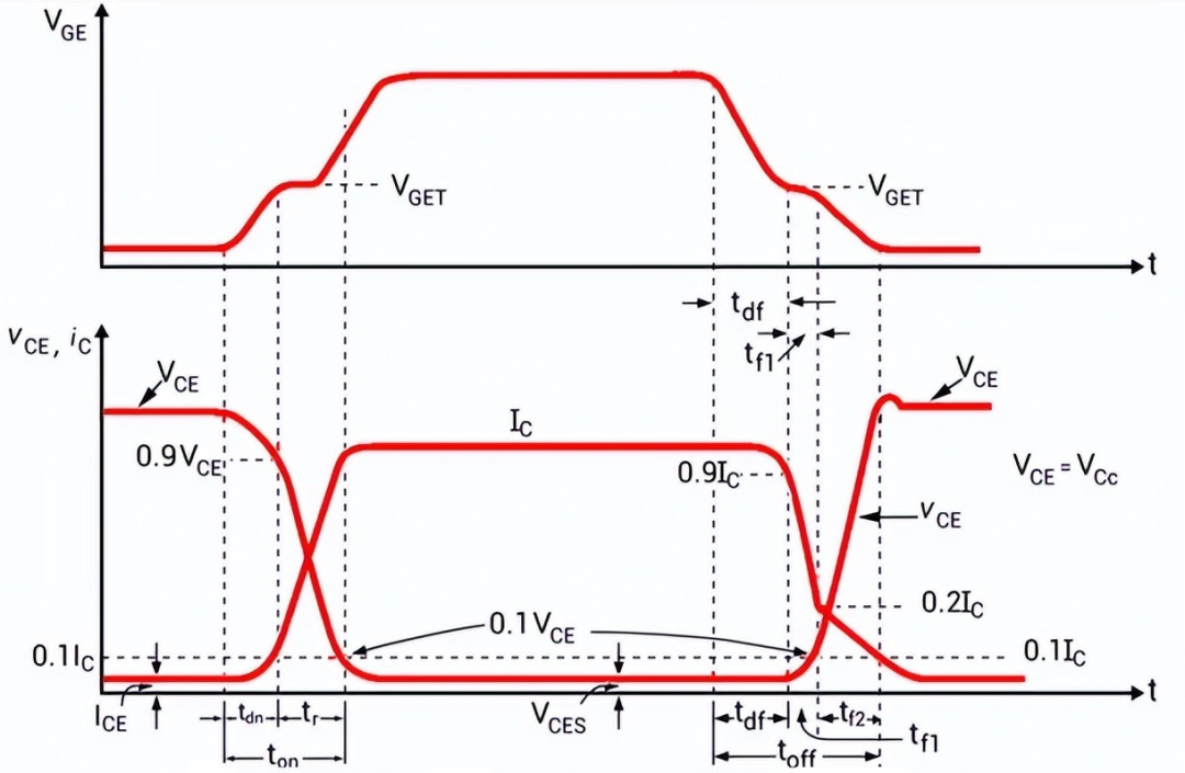
The conduction time (ton) is usually composed of two parts: the delay time (td) and the rise time (tr).
The delay time (td) is defined as the time for the collector current to rise from the leakage current ICE to 0.1IC (the final collector current) and for the collector-emitter voltage to drop from VCE to 0.9VCE when the gate voltage is applied.
The rise time (tr) is defined as the time for the collector current to rise from 0.1IC to IC and for the collector-emitter voltage to drop from 0.9VCE to 0.1VCE.
The turn-off time (toff) is composed of three parts: the delay time (tdf), the initial fall time (tf1), and the final fall time (tf2).
The delay time (tdf) is defined as the time for the collector current to drop from IC to 0.9IC and for VCE to start rising.
The initial fall time (tf1) refers to the time for the collector current to drop from 0.9IC to 0.2IC and for the collector-emitter voltage to rise to 0.1VCE.
The final fall time (tf2) is defined as the time for the collector current to drop from 0.2IC to 0.1IC and for 0.1VCE to rise to the final value VCE.
Off Time Formula
On-time formula
7. IGBT characteristics--input characteristics
The input characteristics of IGBT are clearly shown in the figure below. At the beginning, when there is no voltage applied to the gate pin, IGBT is in the off state, and there is no current flowing through the collector pin. When the voltage applied to the gate pin exceeds the threshold voltage, IGBT begins to conduct, and the collector current IG starts to flow between the collector and emitter terminals. As the gate voltage increases, the collector current also increases correspondingly, as shown in the figure below.

8. IGBT characteristics - output characteristics
Due to the working principle of the IGBT relying on voltage, only a small amount of voltage needs to be provided at the gate terminal to maintain conduction.
Unlike bipolar power transistors, which require continuous base current flow in the base region to maintain saturation, IGBT is a unidirectional device that can only switch in the "forward" direction (from collector to emitter).
IGBT is the opposite of MOS transistors, which have a bidirectional current switching process. MOS transistors are controllable in the forward direction, but the reverse voltage is not controlled.
Under dynamic conditions, when the IGBT is turned off, it may experience latch-up current, which occurs when the driving current in the continuous conduction state seems to exceed the critical value. This is something to be aware of.
In addition, when the gate-emitter voltage is below the threshold voltage, a small amount of leakage current flows through the IGBT. At this time, the collector-emitter voltage is almost equal to the power supply voltage, so the four-layer device IGBT operates in the cut-off region.

The output characteristics of the IGBT can be divided into three stages:
The first stage: When the gate voltage VGE is zero, the IGBT is in the off state, which is called the cut-off region.
The second stage: When VGE increases, if it is less than the threshold voltage, there will be a small amount of leakage current flowing through the IGBT, but the IGBT is still in the cut-off region.
The third stage: When VGE increases to exceed the threshold voltage, the IGBT enters the active region, and current begins to flow through the IGBT. As shown in the figure above, the current will increase with the increase of the voltage VGE.
9. Advantages and disadvantages of IGBT
IGBT is a type of semiconductor device that combines the advantages of BJT and MOSFET. IGBT has the following advantages:
1. Higher voltage and current handling capability.
2. Very high input impedance.
3. Can switch very high current using very low voltage.
4. Voltage-controlled device, meaning it has no input current and low input loss.
5. Simple and inexpensive gate drive circuit, reducing gate drive requirements.
6. Can be easily turned on by applying a positive voltage and turned off by applying zero or negative voltage.
7. Very low on-state resistance.
8. High current density, allowing for smaller chip size.
9. Higher power gain than BJT and MOSFET.
10. Higher switching speed than BJT.
11. Can switch high current levels using low control voltage.
12. Enhanced conductivity due to bipolar nature.
13. Safer.
However, IGBT also has some disadvantages:
1. Slower switching speed than MOSFET.
2. Unidirectional, cannot handle AC waveforms without additional circuitry.
3. Cannot block higher reverse voltage.
4. More expensive than BJT and MOSFET.
5. PNPN structure similar to thyristor, it has latching issues.
6. Longer turn-off time compared to PMOSFET.
The above is about the internal structure, working principle, characteristics, advantages and disadvantages of IGBT (insulated gate bipolar transistor)


Company
About UsContact UsTerms & ConditionsPrivacy StatementPayment,Shipping & InvoiceRefund & Return PolicyWarranty PolicyFrequently asked questionHolidays for Chinese Mid-Autumn Festival and National Day in 2023 Copyright © 2022-2024 Power by Chipdatas Trading Limited. All Rights Reserved.