In-depth understanding of the scientific knowledge of photodiodes and phototransistors, hard-core popular science not to be missed!
There is a class of design problems that can be easily solved through human vision, such as determining the correct position of paper in a printer. For humans, it is easy to judge whether the paper is aligned, but for microprocessors, it is not so simple. Mobile phone cameras need to measure ambient light to determine whether the flash needs to be turned on.
To address these issues, photodiodes or phototransistors can be used. These optoelectronic devices are able to convert light (photons) into electrical signals that can be "seen" by microprocessors (or microcontrollers). In this way, object positioning and arrangement can be controlled, light intensity can be determined, and the physical characteristics of materials can be measured based on their interaction with light.
This article will introduce the working principles of photodiodes and phototransistors, as well as basic application knowledge.
1. Common Spectra of Photodiodes and Phototransistors
Phototransistors and photodiodes are sensitive to light waves of various wavelengths. This is crucial for certain design considerations, such as operations that need to be imperceptible to the human eye. Therefore, designers should have an understanding of the characteristics of the spectrum in order to select devices that are compatible with the application requirements.
The spectrum ranges from long-wavelength infrared (IR) to short-wavelength ultraviolet (UV), with visible light falling between the two (as shown in Figure 1).
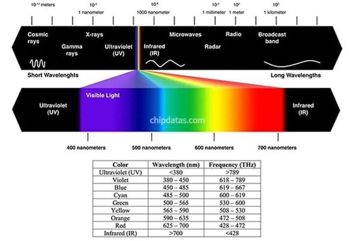
Figure 1 illustrates a portion of the electromagnetic spectrum, including ultraviolet, visible light, and infrared.
The table lists the wavelength range of visible light and its corresponding frequency. (Image source: Once Lighting (top) and Art Pini (bottom))
Most photonic devices are specified using nanometers (nm) as the unit of working wavelength, with frequency values rarely used.
Silicon (Si) photodiodes typically exhibit high sensitivity to visible light. Infrared-sensitive devices, on the other hand, utilize materials such as indium antimonide (InSb), indium gallium arsenide (InGaAs), germanium (Ge), or mercury cadmium telluride (HgCdTe). Additionally, silicon carbide (SiC) is commonly employed in the manufacturing of ultraviolet-sensitive devices.
2. Photodiode
A photodiode is a device with a dual-element P-N or PIN structure that is exposed to light through a transparent material or a cover. When light shines on the structure, the photodiode generates a current or voltage depending on its specific operating mode. There are three operating modes for a photodiode, depending on the applied bias voltage. These modes are photovoltaic mode, photoconductive mode, and avalanche diode mode.
In the absence of an applied bias signal, the photodiode operates in photovoltaic mode and can generate a small output voltage when exposed to a light source. In this mode, the photodiode functions similar to a solar cell. The photovoltaic mode is particularly useful for low-frequency applications and is generally suitable for situations with light intensity below 350kHz and weak light intensity. Due to the low output voltage, an amplifier is often required to amplify the output signal of the photodiode in most cases.
The photoconductive mode requires a reverse bias to be applied to the photodiode. The applied reverse bias voltage creates a depletion region in the P-N structure. The larger the bias voltage, the wider the depletion region. Compared to a diode without bias voltage, a wider depletion region leads to reduced capacitance and faster response time. This operating mode has a higher level of noise, which may need to be controlled through bandwidth limitation.
If the reverse bias voltage is further increased, the photodiode will operate in avalanche diode mode. In this operating mode, the photodiode works under high reverse bias voltage, allowing for multiplication of the number of electron-hole pairs generated by light through the avalanche breakdown effect. This increases the internal gain and sensitivity of the photodiode. This operating mode functions similar to a photomultiplier tube.
In most applications, the photodiode operates in the photoconductive mode with a reverse bias voltage applied (see Figure 2).
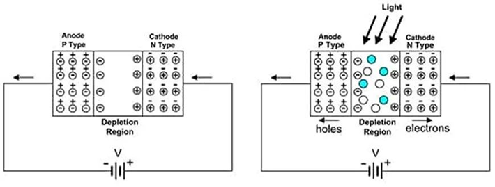
Figure 2: The current generated by a photodiode with a reverse bias voltage applied is proportional to the light intensity due to the generation of electron-hole pairs in the depletion region.
Blue circles represent electrons, white circles represent holes.
In the structure of a non-illuminated photodiode with a reverse bias voltage applied, there is a depletion region with very few free charge carriers. It appears like a charged capacitor. The small current caused by thermal excitation ionization is called "dark" current. An ideal photodiode has zero dark current. The level of dark current and thermal noise is directly proportional to the temperature of the diode. Since the dark current may overshadow the photocurrent at very low light levels, devices with small dark current should be chosen.
When sufficiently energetic light shines on the depletion region, it ionizes atoms in the crystal structure and generates electron-hole pairs. Due to the applied bias voltage, the existing electric field moves electrons to the cathode and holes to the anode, resulting in a photocurrent. The greater the light intensity, the larger the photocurrent. The current-voltage characteristics of a reverse-biased photodiode are shown in Figure 3.

Figure 3: The VI characteristics of a reverse-biased photodiode illustrate the incremental increase in diode current as a function of light intensity.
The graph shows that the reverse current is a function of the applied reverse bias voltage and is proportional to the light intensity. Note that an increase in light intensity leads to a proportional increase in the reverse current level. This is the fundamental principle of using a photodiode to measure light intensity. When the bias voltage exceeds 0.5 volts, it has little effect on the photocurrent. The reverse current can be converted to voltage and processed using a transimpedance amplifier.
3. Types of photodiodes
The diversity of applications in optical detection and measurement has driven the development of various types of photodiodes. The most basic type is the planar P-N junction diode, which performs best in unbiased photovoltaic mode and is also the most cost-effective.
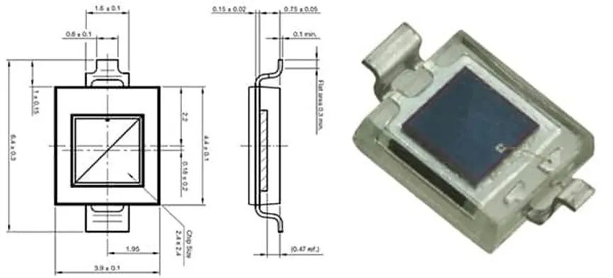
For example, the Advanced Photonix 002-151-001 is a planar diffused InGaAs photodiode/detector (shown in Figure 4). This device is surface-mount device (SMD) packaged with dimensions of 1.6 x 3.2 x 1.1mm and an active optical aperture diameter of 0.05mm. The InGaAs photodiode has a spectral range of 800nm to 1700nm, covering the infrared spectrum. The dark current of the device is less than 1nA, and the spectral responsivity is typically 1A/W, which represents the current output per unit optical power input. This device is suitable for industrial inspection, security, and communication applications.

PIN diodes are formed by adding a high-resistivity intrinsic semiconductor layer between the P-type and N-type layers of a conventional diode, hence the name PIN diode. The insertion of the intrinsic layer increases the effective width of the diode's depletion region, reducing the capacitance and increasing the breakdown voltage. The reduced capacitance effectively improves the speed of the photodiode, while the larger depletion region can generate more photon-induced electron-hole pairs, resulting in higher quantum efficiency.
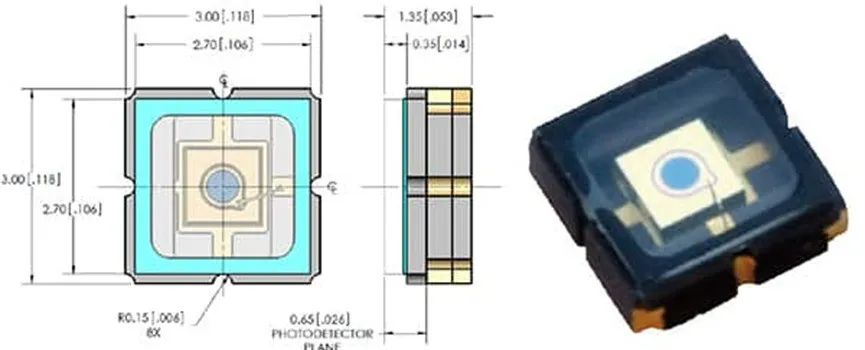
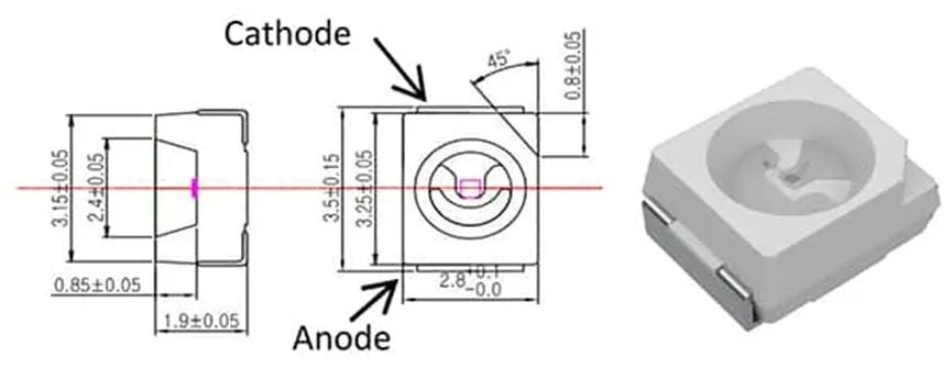
Vishay Semiconductor Opto Division's VBP104SR is a silicon PIN photodiode with a spectral range covering 430nm to 1100nm (from violet to near-infrared). The typical dark current of the device is 2nA, and it features a large optical sensitive area of 4.4mm² (as shown in Figure 5). This device is suitable for high-speed optical detection and other applications.
Avalanche Photodiodes (APDs) function similarly to photomultiplier tubes, utilizing the avalanche effect to generate gain within the diode. Under high reverse bias, each electron-hole pair will generate more electron-hole pairs through the avalanche breakdown effect, resulting in greater gain expressed as "current per photon". Therefore, APDs are an ideal choice for low-light sensitivity applications.
For example, Excelitas Technologies' C30737LH-500-92C is an APD. This device has a spectral range of 500nm to 1000nm (from blue-green to near-infrared), with a peak response wavelength of 905nm (infrared). The spectral responsivity of the device is 60A/W at 900nm, and the dark current is less than 1nA. This device is suitable for high-bandwidth applications such as automotive light detection and ranging (LiDAR) and optical communication (as shown in Figure 6).
4. Schottky Photodiode
A Schottky photodiode is a device based on a metal-semiconductor junction. In this structure, the metal side forms the anode electrode, while the N-type semiconductor side serves as the cathode. Photons pass through a partially transparent metal layer and are absorbed in the N-type semiconductor, releasing pairs of charged carriers. These free charged carriers, under the influence of an applied electric field, escape from the depletion layer, generating a photocurrent.
Another important characteristic of Schottky photodiodes is their extremely fast response time. These devices typically employ small-sized diode structures that can react quickly. Schottky photodiodes with bandwidths in the gigahertz (GHz) range are already available in the market, making them an ideal choice for high-bandwidth optical communication links.
For example, the GUVB-S11SD photodetector from Genicom Co., Ltd is a Schottky photodiode (see Figure 7). This UV-sensitive photodiode is widely used in applications such as UV index measurement. The device utilizes a material based on aluminum gallium nitride (AlGaN), with a spectral sensitivity range from 240nm to 320nm in the ultraviolet spectrum. It exhibits sensitivity to the spectral range while being insensitive to visible light, which is a useful feature in bright environments. The device has a dark current of less than 1nA and a responsivity of 0.11A/W.
5. phototransistor
Phototransistor is a semiconductor device similar to a photodiode, and its output current is proportional to the light intensity. It can be regarded as a photodiode with a built-in current amplifier. It consists of an NPN transistor, where the base connection is replaced by a light source. The base-collector junction is reverse biased and exposed to external light through a transparent window. To maximize the photocurrent, the base-collector junction is designed to be as large as possible. On the other hand, the base-emitter junction is forward biased, and the collector current is proportional to the incident light intensity. The light provides the base current, which is then amplified by the transistor. When there is no light, similar to a photodiode, there is a small dark current flowing.
One type of NPN phototransistor called MTD8600N4-T is produced by Marktech Optoelectronics. Its spectral sensitivity range is from 400nm to 1100nm (visible light to near-infrared), with a peak response at 880nm (see Figure 8).
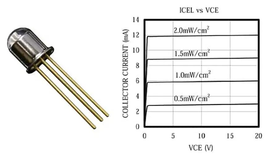
Figure 8 shows the relationship between the collector current generated by the MTD8600N4-T phototransistor and the incident light intensity, which is proportional. It is important to note that due to the current amplification effect of the transistor, the collector current is one order of magnitude higher than that of a photodiode. (Image source: Marktech Optoelectronics)
This phototransistor is packaged in a metal can with a transparent dome. The figure illustrates that the collector current is a function of the collector-to-emitter voltage with light irradiance as a parameter. Due to the current amplification effect of the transistor, the collector current is significantly higher than the current in a photodiode.
6. summary
The use of phototransistors and photodiodes for light detection provides an important means for microprocessors or microcontrollers to understand the physical world and perform corresponding control or analysis algorithms. Phototransistors and photodiodes have similarities in their applications, but each has its own unique advantages. Phototransistors have a higher output current level compared to photodiodes, while photodiodes exhibit better performance at higher frequencies.


Company
About UsContact UsTerms & ConditionsPrivacy StatementPayment,Shipping & InvoiceRefund & Return PolicyWarranty PolicyFrequently asked questionHolidays for Chinese Mid-Autumn Festival and National Day in 2023 Copyright © 2022-2024 Power by Chipdatas Trading Limited. All Rights Reserved.