


 Purchase Protection
Powerful Protection from Payment to Delivery
Secure and Reliable Payment
Money Back Guarantee
Shipping and Delivery
After-Sales Service
Enter the order reference number received by email to check the status or make payment.
Fan-out packaging is becoming ubiquitous
With the development of semiconductor technology, Moore's law has become difficult to maintain the previous speed below 7 nanometers. Therefore, backend packaging technology has become increasingly important to meet the demand for low latency, higher bandwidth, and cost-effective semiconductor chips. In this regard, fan-out packaging is becoming the preferred choice for addressing heterogeneous integration challenges due to its ability to provide larger chips with higher I/O density, significantly reducing system size.
The rise of fan-out packaging
Fan-out (FO) and fan-in (FI) are two electronic packaging technologies that follow similar process flows. After processing and cutting the chip, the chip is placed on a reconstituted wafer, which is based on an epoxy resin molded compound. Then, a redistribution layer (RDL) is formed on the molded compound, which is a metal copper interconnect that electrically connects various parts of the package. Finally, the individual package on the reconstituted wafer is cut.
In fan-in packaging, RDL is wired inward, while in fan-out packaging, RDL can be wired both inward and outward. As a result, fan-in packaging can only accommodate up to about 200 I/O, while fan-out packaging can achieve more I/O.
The earliest fan-out packaging was proposed by Infineon in 2004, called fan-out wafer level packaging (FOWLP), which began commercial production in 2009. However, FOWLP was only applied to mobile baseband chips and quickly reached market saturation. It was not until 2016 that TSMC developed integrated fan-out (InFO) packaging based on FOWLP, which was used for the A10 application processor in the Apple iPhone 7 series. The combination of these two technologies greatly promoted the development of fan-out packaging.
Today, the fan-out packaging market is experiencing strong growth. According to Yole's report, the fan-out packaging market will reach billions of dollars in the coming years. The overall CAGR is expected to reach 15.1% between 2020-2026, and the market size will increase to $3.425 billion by the end of 2026. Among them, the mobile and consumer sectors are $1.613 billion, telecommunications and infrastructure are $1.597 billion, and the automotive and travel sectors are $216 million.
two flowers
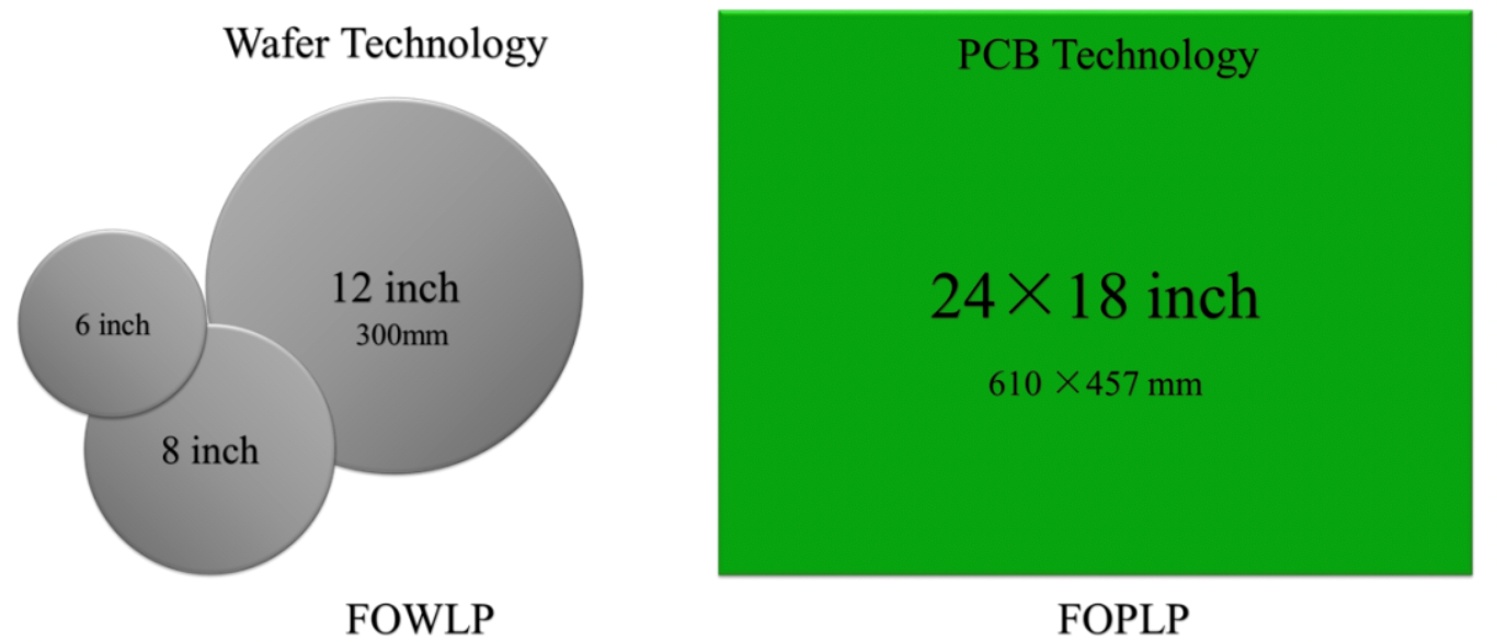
Fan-out Wafer Level Packaging (FOWLP) and Fan-out Panel Level Packaging (FOPLP) are two important branches of fan-out packaging technology.
FOPLP technology was initially a substrate-embedded packaging technology that embeds some passive or power devices into the substrate for RDL interconnection, forming a miniaturized solution. Compared to FOWLP, FOPLP has a larger package size and lower cost, so it quickly became a research and development hotspot in the packaging field. FOWLP is mainly used for large chips such as CPUs, GPUs, and FPGAs, while FOPLP is mainly used for APE, PMIC, power devices, etc.
FOPLP uses a large carrier board, such as a 24×18 inch (610×457mm) PCB carrier board, which is approximately 4 times the area of a 300mm silicon wafer, so it can be simply regarded as a way to produce 4 times advanced packaging products under one process.
The development of FOWLP is mainly driven by TSMC's provision of InFO to the IOS ecosystem. Now, more and more top smartphone OEM manufacturers will adopt HDFO (High-Density Fan Out) design. However, FOWLP is still a niche technology, with only a few participants such as TSMC, Samsung, and ASE. Because its competitors, fan-in WLCSP and FCCSP, still maintain advantages such as low cost and high reliability, the growth of FOWLP will not be particularly fast.
The adoption of 5G mmWave may help increase the number of FOWLPs, especially for the OSAT sub-market (RF sub-market). With more and more smartphone OEM manufacturers hoping to adopt the HDFO platform for application processors, FOWLP capital expenditures are expected to grow.
There is still a lot of uncertainty in the FOWLP market, which requires new integrated solutions and high-performance fan-out packaging solutions. However, this market has great market potential. Mainstream packaging factories and TSMC already have their own FOWLP technology, but they are named differently.
FOPLP can be regarded as a solution that converts from wafer and strip level to larger size panel level. Like the FOWLP process, FOPLP technology can integrate the pre- and post-packaging processes, and can be regarded as a one-time packaging process. Due to its potential cost-effectiveness and higher manufacturing efficiency, it has attracted widespread attention in the market. In addition, the large size of the panel and the higher carrier utilization rate (95%) bring far greater economies of scale than FOWLP and can achieve mass production of large-scale packaging.
Due to the success and market awareness of FOWLP, FOPLP has attracted more attention, including many manufacturers with different business models, such as outsourced semiconductor assembly and testing manufacturers, IDM, foundries, substrate manufacturers, and flat panel display (FPD) manufacturers. They all strive to enter the advanced packaging business through FOPLP technology.
FOPLP has two technical routes. One is to use this technology for Samsung's AP processor, which requires very strong customer support. The other is to use substrate-like process paths to achieve board-level packaging for products such as MOSFETs that were originally QFNs, which is more suitable for ordinary manufacturers.
According to Yole's report, FOWLP still accounts for the absolute mainstream of fan-out packaging, with a market share of 97% in 2020. However, FOPLP will also grow steadily, and its market share will increase from 3% in 2020 to 7% in 2026.
Whether it is FOWLP or FOPLP, heterogeneous integration of various chips in fan-out packaging, how to arrange them on the PCB reasonably and achieve efficient electrical connection, and how to form high film thickness uniformity and high resolution RDL are all key challenges that need to be faced.
Manufacturers from all walks of life are competing to lay out
Taiwan Semiconductor Manufacturing Company (TSMC) is the leader in the FOWLP market, mainly due to the successful use of inFO packaging in Apple's APE. This led to the emergence of a new sub-segment in 2016 - HDFO (High-Density Fan-Out) - which TSMC has capitalized on. InFO-oS technology is now being used in HPCs in small-scale manufacturing, and InFO-MS (Memory on Substrate) has been developed for servers, while InFO-AiP has been developed for 5G. With both wafer foundry and high-end packaging capabilities, TSMC is well-positioned to continue creating unique value.
Currently, TSMC holds a 66.9% market share in this field. When combined with the market share of other players such as United Microelectronics Corporation (UMC), Jiangsu Changjiang Electronics Technology (JCET), and Amkor Technology, these four companies hold a total market share of 95%.
Packaging companies in mainland China are also actively developing fan-out packaging and have developed new processes with unique features. For example, JCET has developed the ECP process, which uses encapsulated film instead of liquid or powder encapsulants. Huatian Technology has introduced eSiFO technology, which uses via-last TSV to achieve high-density 3D interconnects.
In the FOPLP segment, Samsung Electronics is the absolute leader. Samsung initially invented this technology to compete with TSMC's inFO.
Samsung Group has played an important role in design, memory, logic, packaging, chip assembly, and final products, so it can drive breakthroughs in fan-out packaging internally. As part of the Samsung Group, Samsung Electro-Mechanics must contribute differentiated but cost-effective technology. In 2018, Samsung Electro-Mechanics achieved a new milestone by introducing APE-PMIC equipment with ePLP (embedded Panel-Level Packaging) PoP technology for the Samsung Galaxy Watch. Samsung Electro-Mechanics will continue to innovate cost-effective high-density fan-out packaging to compete with TSMC in Apple's packaging and front-end business.
In addition to Samsung Electro-Mechanics, packaging companies such as J-DEVICES, FUJIKURA, UMC, Deca Technologies, and SPIL are also actively investing in FOPLP processes. In mainland China, companies such as Hefei Silan Microelectronics, SK Hynix, and Chongqing Silicon Power Microelectronics have also achieved mass production.
It seems that both FOWLP and FOPLP have their own development paths. However, the development of FOPLP has given packaging companies, as well as substrate manufacturers and flat panel display (FPD) manufacturers, the capital to compete with wafer foundries in the fan-out packaging field. In my opinion, when FOPLP technology matures further and more types of companies participate, fan-out packaging will experience a comprehensive outbreak.

Company
About UsContact UsTerms & ConditionsPrivacy StatementPayment,Shipping & InvoiceRefund & Return PolicyWarranty PolicyFrequently asked questionHolidays for Chinese Mid-Autumn Festival and National Day in 2023 Copyright © 2022-2024 Power by Chipdatas Trading Limited. All Rights Reserved.