


 Purchase Protection
Powerful Protection from Payment to Delivery
Secure and Reliable Payment
Money Back Guarantee
Shipping and Delivery
After-Sales Service
Enter the order reference number received by email to check the status or make payment.
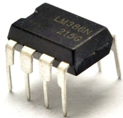
Design of audio amplifier circuit based on LM386
1. Overview of Audio Power Amplifier
1.1 Product Features
An audio power amplifier, also known as a power amp, provides a certain output power to the load RL (loudspeaker) of an audio amplifier. When the load is fixed, the goal is to maximize the output power, minimize the non-linear distortion of the output signal, and achieve high efficiency.
1.2 Performance Indicators
Signal-to-Noise Ratio (S/N): Also known as the SNR, it represents the contrast between the useful component of the signal and the strength of the noise, often expressed in decibels. A higher signal-to-noise ratio indicates less generated noise.
Sensitivity: For amplifiers, sensitivity generally refers to the voltage magnitude of the input signal when reaching the rated output power or voltage. Therefore, it is also known as input sensitivity. For loudspeakers, sensitivity refers to the sound pressure level in decibels produced at a distance of 1 meter in front of the speaker when applying 1W of input power.
Damping Factor: The ratio of the load impedance to the amplifier's output impedance. Using negative feedback, the output impedance of transistor amplifiers is extremely low, typically only a few ohms or even smaller, resulting in damping factors ranging from tens to hundreds.
Dynamic Range: The level difference between the strongest and weakest parts of a signal. For equipment, the dynamic range represents its ability to handle both strong and weak signals.
Response: Frequency Response, also known as frequency response, measures the ability of a device to reproduce signals evenly across the high, mid, and low frequency ranges. There are two requirements for frequency response: first, the range should be as wide as possible, with a low lower limit and a high upper limit; second, the response at each point within the frequency range should be as flat as possible, avoiding significant fluctuations.
Shielding: The technique of covering electronic devices or wires with materials that are conducive to conducting electromagnetic waves in order to prevent interference from external electromagnetic noise on useful signals.
1.3 Production Cost
The circuit is simple, and the cost is not high.
1.4 Application Fields
Class A amplifiers have the least distortion, the lowest efficiency, and the highest heat generation. It is difficult to achieve high power output. Class AB amplifiers amplify the positive and negative half cycles separately (push-pull), introducing various types of distortion but with high efficiency. Class A operation is used for small signals, while Class AB operation is used for large signals, striking a balance between distortion and efficiency. This is currently the mainstream type of power amplifier. By designing the circuit properly and selecting high-quality components, it is possible to achieve high performance. Class D amplifiers, also known as digital amplifiers, have extremely high efficiency and relatively high technical specifications. They are widely used in small electronic products, such as car audio systems. However, Class D amplifiers have not yet gained widespread recognition among audiophiles.
2. Circuit Design
2.1 Schematic Design
Design requirements: When the load is fixed, the goal is to maximize the output power, minimize the nonlinear distortion of the output signal, achieve high efficiency, and generate a real, efficient, and low-distortion input audio signal at the desired volume and power level on the sound output device.
Design steps:
First, design the circuit based on the desired chip for the functionality.
Second, understand the properties and characteristics of the chip.
Third, use DXP software to draw the circuit schematic.

In the LM386 chip, pin 2 is the inverting input, pin 3 is the non-inverting input, pin 5 is the output, pins 6 and 4 are the power and ground respectively, and pins 1 and 8 are the voltage gain setting pins. When in use, a bypass capacitor is typically connected between pin 7 and ground, usually with a value of 10μF.
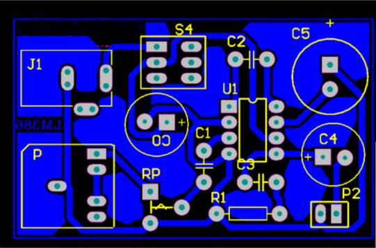
2.2 Printed Circuit Board (PCB) Design
Based on the schematic, create the PCB and perform the layout.


Company
About UsContact UsTerms & ConditionsPrivacy StatementPayment,Shipping & InvoiceRefund & Return PolicyWarranty PolicyFrequently asked questionHolidays for Chinese Mid-Autumn Festival and National Day in 2023 Copyright © 2022-2024 Power by Chipdatas Trading Limited. All Rights Reserved.