An article to understand fan-out wafer-level packaging (FOWLP)
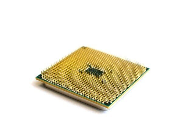
In recent years, as the feature size of chips approaches the physical limit, advanced packaging technology has become an important way to continue Moore's Law. In this field, fan-out wafer-level packaging (FOWLP) technology has attracted much attention because it provides solid and powerful support for the next generation of compact and high-performance electronic devices.
Compared with traditional packaging technology, FOWLP technology can achieve heterogeneous integration of smaller chips without the use of intermediate layers or through-silicon vias (TSV). When embedding each bare die, there is an additional I/O connection point between the gaps, which not only increases the number of I/Os but also improves the utilization of silicon. In addition, FOWLP technology can maximize interconnect density by achieving seamless connections between two to five micrometer spacing lines.
Therefore, FOWLP technology is considered one of the important trends in future packaging technology. It can provide higher performance and smaller size for the next generation of electronic devices, while also improving the utilization of silicon and interconnect density. With the continuous development and improvement of this technology, it is believed that it will play an increasingly important role in future electronic devices.
Process steps
The completed wafers produced by the foundries are tested and then enter the production line. Similar to traditional packaging, the first step in fan-out packaging is to cut the incoming wafer into bare chips.
The main feature of fan-out packaging is to combine the cut bare chips into a reconstructed wafer. Compared with the incoming wafer, the distance between the bare chips on the reconstructed wafer is relatively larger, which facilitates the construction of chip products with larger unit area and more input/output (I/O).
Laminate and remove slides
After the reconstruction wafer is packaged, it needs to be encapsulated to fix and protect the bare chip. This step is crucial because it can ensure the stability and reliability of the reconstructed wafer. After encapsulation is completed, the carrier needs to be removed to expose the input and output interfaces (I/O) of the bare chip to the outside for subsequent testing and use.

make redistribution layer
For the convenience of soldering, the interfaces (I/O) on the bare die need to be led out to a convenient location at the edge of the wafer. This process requires the fabrication of a redistribution layer (RDL) on the wafer using metal wire technology. Through the RDL layer, the signal leads on the bare die can be transferred to the edge of the wafer, making it easier to perform subsequent soldering work. To ensure the reliability and stability of the signal, this process requires high-precision process control.
Wafer Thinning
In order to make the finished chip thinner, it is necessary to thin the wafer.
Ball planting
Ball planting is performed on the metal pads of the redistribution layer (RDL) connection so that subsequent chips can be easily soldered on the printed circuit board (PCB).
Wafer dicing, finished chip
The final step involves restructuring and cutting the wafer to obtain independent chips.


Company
About UsContact UsTerms & ConditionsPrivacy StatementPayment,Shipping & InvoiceRefund & Return PolicyWarranty PolicyFrequently asked questionHolidays for Chinese Mid-Autumn Festival and National Day in 2023 Copyright © 2022-2024 Power by Chipdatas Trading Limited. All Rights Reserved.