- Deliver to
 USLanguageEnglish


Quick Links
Order search and payment
Enter the order reference number received by email to check the status or make payment.
 Purchase Protection
Powerful Protection from Payment to Delivery
Secure and Reliable Payment
Money Back Guarantee
Shipping and Delivery
After-Sales Service
All product names, trademarks, brands, and logos on this site are the property of their respective owners. Their use is for identification purposes only and does not imply any affiliation or authorization from the rights holders. We are not authorized dealers or distributors of the brand. The warranty is provided by us, not the original manufacturer.
Product Details
Manufacturer
Lattice Semiconductor
Product Category
FPGAs (Field Programmable Gate Array)
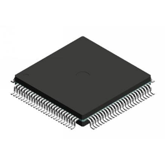
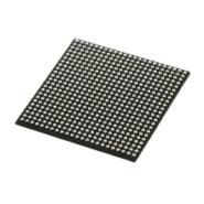
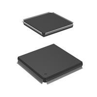
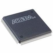
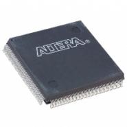
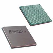
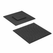
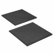
OR2T15A-6S208 - Brand New Lattice Semiconductor FPGAs (Field Programmable Gate Array)
Brand:Lattice Semiconductor
Manufacturer Part No.:OR2T15A-6S208
Variations
Quantity
Shipping:
Free ShippingEstimated 15-30 business days via Registered Air Mail or othersSee details
Delivery:
Estimated between Wed, Mar 25 and Fri, Mar 27.This item requires 2-5 business days for processing before shipping after payment is confirmed. And depending on the destination and shipping method.See details
Return:60 days returns. Buyer pays for return shipping.See details
Payments:


Shop with confidence
One-month free return and one year warranty.
Full or Partial Refund , If the item is not as described
Full Refund if you don't receive your order
Explore related items


The tension in logistics has eased and normal shipping has resumed. All orders shipments will be sent out within 1-2 days.
Company
About UsContact UsTerms & ConditionsPrivacy StatementPayment,Shipping & InvoiceRefund & Return PolicyWarranty PolicyFrequently asked questionHolidays for Chinese Mid-Autumn Festival and National Day in 2023 Copyright © 2022-2024 Power by Chipdatas Trading Limited. All Rights Reserved.