⚠ All product names, trademarks, brands, and logos on this site are the property of their respective owners. Their use is for identification purposes only and does not imply any affiliation or authorization from the rights holders. We are not authorized dealers or distributors of the brand. The warranty is provided by us, not the original manufacturer.
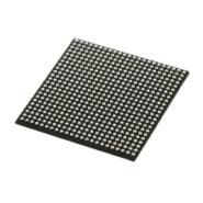
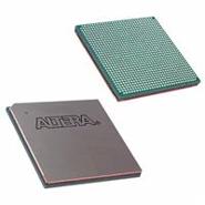
OR3T306S208I-DB
OR3T306S208I-DB - Brand New Lattice Semiconductor FPGAs (Field Programmable Gate Array)


 Credit Card
 - One-month free return and one year warranty.
- Full or Partial Refund, if the item is not as described
- Full Refund if you don't receive your order
Description
FPGA Overview
The ORCA Series 3 FPGAs are a new generation of SRAM-based FPGAs built on the
successful OR2C/TxxA FPGA Series from Lucent Technologies Microelectronics
Group, with enhancements and innovations geared toward today’s high-speed
designs and tomorrow’s systems on a single chip. Designed from the start to be
synthesis friendly and to reduce place and route times while maintaining the
complete routability of the ORCA 2C/2T devices, Series 3 more than doubles the
logic available in each logic block and incorporates system-level features
that can further reduce logic requirements and increase system speed. ORCA
Series 3 devices contain many new patented enhancements and are offered in a
variety of packages, speed grades, and temperature ranges.
Features
■ High-performance, cost-effective, 0.35 µm (OR3C) and 0.3 µm (OR3T) 4-level
metal technology, (4- or 5-input look-up table delay of 1.1 ns with -7 speed
grade in 0.3 µm).
■ Same basic architecture as lower-voltage, advanced process technology Series
3 architectures. (See ORCA Series 3L FPGA documentation.)
■ Up to 186,000 usable gates.
■ Up to 452 user I/Os. (OR3Txxx I/Os are 5 V tolerant to allow interconnection
to both 3.3 V and 5 V devices, selectable on a per-pin basis.)
■ Pin selectable I/O clamping diodes provide 5 V or 3.3 V PCI compliance and 5
V tolerance on OR3Txxx devices.
■ Twin-quad programmable function unit (PFU) architecture with eight 16-bit
look-up tables (LUTs) per PFU, organized in two nibbles for use in nibble- or
byte-wide functions. Allows for mixed arithmetic and logic functions in a
single PFU.
■ Nine user registers per PFU, one following each LUT, plus one extra. All
have programmable clock enable and local set/reset, plus a global set/reset
that can be disabled per PFU.
■ Flexible input structure (FINS) of the PFUs provides a routability
enhancement for LUTs with shared inputs and the logic flexibility of LUTs with
independent inputs.
■ Fast-carry logic and routing to adjacent PFUs for nibble-, byte-wide, or
longer arithmetic functions, with the option to register the PFU carry-out.
■ Softwired LUTs (SWL) allow fast cascading of up to three levels of LUT logic
in a single PFU for up to 40% speed improvement.
■ Supplemental logic and interconnect cell (SLIC) provides 3-statable buffers,
up to 10-bit decoder, and PAL*-like AND-OR with optional INVERT in each
programmable logic cell (PLC), with over 50% speed improvement typical.
■ Abundant hierarchical routing resources based on routing two data nibbles
and two control lines per set provide for faster place and route
implementations and less routing delay.
■ TTL or CMOS input levels programmable per pin for the OR3Cxx (5.0 V)
devices.
■ Individually programmable drive capability: 12 mA sink/6 mA source or 6 mA
sink/3 mA source.
■ Built-in boundary scan (IEEE †1149.1 JTAG) and TS_ALL testability function
to 3-state all I/O pins.
■ Enhanced system clock routing for low skew, high-speed clocks originating
on-chip or at any I/O.
■ Up to four ExpressCLK inputs allow extremely fast clocking of signals on-
and off-chip plus access to internal general clock routing.
■ StopCLK feature to glitchlessly stop/start ExpressCLKs independently by user
command.
■ Programmable I/O (PIO) has:
— Fast-capture input latch and input flip-flop (FF) latch for reduced input
setup time and zero hold time.
— Capability to (de)multiplex I/O signals.
— Fast access to SLIC for decodes and PAL-like functions.
— Output FF and two-signal function generator to reduce CLK to output
propagation delay.
— Fast open-drain dive capability
— Capability to register 3-state enable signal.
■ Baseline FPGA family used in Series 3+ FPSCs (field programmable system
chips) which combine FPGA logic and standard cell logic on one device.
Shipping
| First item | Additional item | Service | Description |
|---|---|---|---|
| $0.00 | Free | Free Shipping | Estimated 15-30 business days via Registered Air Mail or others |
| $27.50 | Free | Expedited Shipping | Estimated delivery time is 3-5 business days, with some areas possibly taking 6-9 business days depending on the shipping address. The main courier companies include but are not limited to UPS, DHL, and FedEx. |
| $0.00 | Free | Buyer cooperating carrier | Using buyer's cooperating carrier. Buyer should create a shipping label and share it to us. And then we will call carrier for pickup |
| $38.00 | Free | Expedited Shipping | Estimated delivery time is 3-5 business days, with some areas possibly taking 6-9 business days depending on the shipping address. The main courier companies include but are not limited to UPS, DHL, and FedEx. |
Delivery
- The transportation time may be delayed due to customs clearance, local holidays or abnormal events.
- The estimated time is based on the fastest speed provided by commercial couriers (DHL, FedEx, UPS etc).
- The estimated time does not include the lead time of the item. The lead time of most items is 2–5 business days. If more than 5 working days are needed, we will manually confirm with you.
| Flag | Country | Express Delivery | Standard Delivery |
|---|---|---|---|
 | United States | 3 - 5 days | 10-15 days |
 | Canada | 3 - 5 days | 10-20 days |
 | Mexico | 3 - 5 days | 10-17 days |
 | Germany | 3 - 5 days | 10-12 days |
 | Italy | 3 - 5 days | 10-15 days |
 | United Kingdom | 3 - 5 days | 10-12 days |
Estimated Delivery
This item requires 2-5 business days for processing before shipping after payment is confirmed. And depending on the destination and shipping method.
Return Policy
| Return window | Refund type | Return shipping |
|---|---|---|
| 60 days after receiving item | Money Back or Replacement | Buyer pays for return shipping |
电子元器件与工控产品的真实买家评价
 In Stock
 5CEFA5F23I7N
5CEFA5F23I7N - Brand New Intel / Altera FPGAs (Field Programmable Gate Array)
 In Stock
 APA075-PQG208
APA075-PQG208 - Brand New Microchip Technology FPGAs (Field Programmable Gate Array)
 In Stock
 APA600-PQG208M
APA600-PQG208M - Brand New ACTEL FPGAs (Field Programmable Gate Array)
 In Stock
 EP1C12Q240C8N
EP1C12Q240C8N - Brand New Intel / Altera FPGAs (Field Programmable Gate Array)
 In Stock
 EP1K100QC208-1
EP1K100QC208-1 - Brand New Intel / Altera FPGAs (Field Programmable Gate Array)
 In Stock
 EP1SGX25DF1020C6N
EP1SGX25DF1020C6N - Brand New Intel / Altera FPGAs (Field Programmable Gate Array)
 In Stock
 EP2AGX45DF25I3N
EP2AGX45DF25I3N - Brand New Intel / Altera FPGAs (Field Programmable Gate Array)
 In Stock
 EP2C35F484C6N
EP2C35F484C6N - Brand New Intel / Altera FPGAs (Field Programmable Gate Array)
 In Stock
 EP2C5T144C8N
EP2C5T144C8N - Brand New Intel / Altera FPGAs (Field Programmable Gate Array)
 In Stock
 EP2C5T144I8N
EP2C5T144I8N - Brand New Intel / Altera FPGAs (Field Programmable Gate Array)