MT29C1G12MAVRAJA-6IT - Brand New MARVELL IC Chips
-
Description
Micron NAND Flash devices include an asynchronous data interface for high-performance I/O operations. These devices use a highly multiplexed 8-bit bus (I/Ox) to transfer commands, address, and data. There are five control signals used to implement the asynchronous data interface: CE#, CLE, ALE, WE#, and RE#. Additional signals control hardware write protection and monitor device status (R/B#). This hardware interface creates a low pin-count device with a standard pinout that remains the same from one density to another, enabling future upgrades to higher densities with no board redesign. A target is the unit of memory accessed by a chip enable signal. A target contains one or more NAND Flash die. A NAND Flash die is the minimum unit that can independently execute commands and report status. This device has an internal 4-bit ECC that can be enabled using the GET/SET features. See Internal ECC and Spare Area Mapping for ECC for more information.
Specifications and Features
- Open NAND Flash Interface (ONFI) 1.0-compliant1
- Single-level cell (SLC) technology
- Organization
- Page size x8: 2112 bytes (2048 + 64 bytes)
- Page size x16: 1056 words (1024 + 32 words)
- Block size: 64 pages (128K + 4K bytes)
- Plane size: 2 planes x 2048 blocks per plane
- Device size: 4Gb: 4096 blocks; 8Gb: 8192 blocks 16Gb: 16,384 blocks
- Asynchronous I/O performance
- tRC/tWC: 20ns (3.3V), 25ns (1.8V)
- Array performance
- Read page: 25µs 3
- Program page: 200µs (TYP: 1.8V, 3.3V)3
- Erase block: 700µs (TYP)
- Command set: ONFI NAND Flash Protocol
- Advanced command set
- Program page cache mode4
- Read page cache mode 4
- One-time programmable (OTP) mode
- Two-plane commands 4
- Interleaved die (LUN) operations
- Read unique ID
- Block lock (1.8V only)
- Internal data move
- Operation status byte provides software method for detecting
- Operation completion
- Pass/fail condition
- Write-protect status
- Ready/Busy# (R/B#) signal provides a hardware method of detecting operation completion
- WP# signal: Write protect entire device
- First block (block address 00h) is valid when shipped from factory with ECC. For minimum required ECC, see Error Management.
- Block 0 requires 1-bit ECC if PROGRAM/ERASE cycles are less than 1000
- RESET (FFh) required as first command after power-on
- Alternate method of device initialization (Nand_Init) after power up (contact factory)
- Internal data move operations supported within the plane from which data is read
- Quality and reliability
- Data retention: 10 years
- Endurance: 100,000 PROGRAM/ERASE cycles
- Operating voltage range
- VCC: 2.7–3.6V
- VCC: 1.7–1.95V
- Operating temperature:
- Commercial: 0°C to +70°C
- Industrial (IT): –40ºC to +85ºC
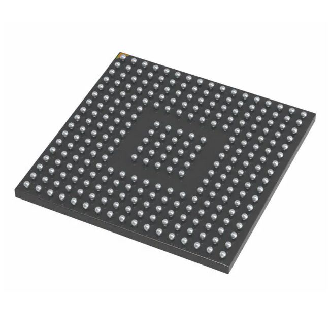
- Package
- 48-pin TSOP type 1, CPL2
- 63-ball VFBGAApplication Scenarios
This model can be used in various applications such as IC chips, electronic devices, and memory storage devices.
Comparison
Advantages:
- High-performance I/O operations
- Low pin-count device
- Standard pinout for easy upgrades to higher densities
- Internal 4-bit ECC
- Wide operating voltage range
Disadvantages:
- Restricted to specific protocols
- Requires additional hardware signals for control and monitoring
- Specific requirements for ECC and initialization
- Restricted to specific temperature ranges
-
Similar parts: 430483 , Click to view
-
Datasheet
-
Shopping guide
Delivery period:
- - Will ship out in 2-3 days
- - DHL Express: 3-7 business days
- - DHL eCommerce: 12-22 business days
- - FedEx International Priority: 3-7 business days
- - EMS: 10-15 business days
Shipping fee:
- - Automatic Email notification (above 5 times)
- - View in your order page
Shipping option:
DHL, FedEx, EMS, SF Express, and Registered Air MailShipping tracking:
- - Automatic Email notification (above 5 times)
- - View in your order page
How to Buy:
- - In-stock, Add to cart > Check out > Submit order > Complete payment >Delivery.
- - Inquiry, Add to inquiry sheet/Submit bom/inquire file/Send email us > Quote > Place order > Complete payment >Delivery.
- View more
Payment:
- - Paypal,Credit Card includes Visa, Master, American Express.
- - Wire transfer, include Local bank transfer.
- - Western Union.
- View more
-
Popular parts of the same kind
- Datasheet: Download MT29C1G12MAVRAJA-6IT
- Chipdatas Part: CD90-MT29C1G12MAVRAJA-6IT
- Warehouse: China, Hong Kong
- Dispatch: Within 24 hours
- Free Shipping: Yes
- Prority Shipping: Yes, 3-5 days
- Last Updated: 2024/09/30 04:17 +0800
-
- Full Refund if you don't receive your order
- Full or Partial Refund , If the item is not as described
-
 E-STLC2500CTR - Brand New STMicroelectronics IC ChipsWFBGA
 -
 CY7C68053A-56BA - Brand New Cypress Semiconductor IC ChipsBGA
 -
 AR8035-AL1A-R - Brand New QCA IC ChipsBGA
 -
 BL1117-ADC - Brand New Belling IC ChipsSOT-223
 -
 HM628512BLFP-7 - Brand New Nexperia IC ChipsSOP-32
 -
 BCM5325FKQMG - Brand New Broadcom IC ChipsQFP
 -
 D431000AGW-70LL - Brand New NEC IC ChipsSOP
 -
 HT46R003B - Brand New HOLTEK IC ChipsSOP-16
 -
 BCM2045KWBG - Brand New Broadcom IC ChipsBGA
 -
 H26M52103FMR - Brand New Skhynix IC ChipsBGA
-
The fee is charged according to the rule of PayPal.
-
The fee is charged according to the rule of PayPal.
-
Western Union charge US$0.00 banking fee.
-
We recommend to use bank transfer for large orders to save on handling fees.
-
DHL(www.dhl.com)
$40 limited time offer. -
UPS(www.ups.com)
$40 limited time offer. -
FedEx(www.fedex.com)
$40 limited time offer. -
Registered Mail(www.singpost.com)
Free shipping without minimum order.
