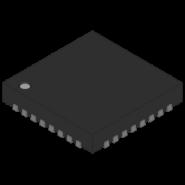
ISPGAL22V10AB-75LN - Brand New LATTICE Programmable Logic Device (CPLDs/FPGAs)
-
Introduction
The ispGDX2™ family is Lattice’s second generation in-system programmable generic digital crosspoint switch for high speed bus switching and interface applications.
The ispGDX2 family is available in two options. The standard device supports sysHSI capability for ultra fast serial communications while the lower-cost “E-series” supports the same high-performance FPGA fabric without the sysHSI Block.
This family of switches combines a flexible switching architecture with advanced sysIO interfaces including high performance sysHSI Blocks, and sysCLOCK PLLs to meet the needs of the today’s high-speed systems. Through a muliplexer-intensive architecture, the ispGDX2 facilitates a variety of common switching functions.Features
■ High Performance Bus Switching
• High bandwidth
– Up to 12.8 Gbps (SERDES)
– Up to 38 Gbps (without SERDES)
• Up to 16 (15x10) FIFOs for data buffering
• High speed performance
– fMAX = 360MHz
– tPD = 3.0ns
– tCO = 2.9ns
– tS = 2.0ns
• Built-in programmable control logic capability
• I/O intensive: 64 to 256 I/Os
• Expanded MUX capability up to 188:1 MUX
■ sysCLOCK™ PLL
• Frequency synthesis and skew management
• Clock multiply and divide capability
• Clock shifting up to +/-2.35ns in 335ps steps
• Up to four PLLs
■ sysIO™ Interfacing
• LVCMOS 1.8, 2.5, 3.3 and LVTTL support for standard board interfaces
• SSTL 2/3 Class I and II support
• HSTL Class I, III and IV support
• GTL+, PCI-X for bus interfaces
• LVPECL, LVDS and Bus LVDS differential support
• Hot socketing
• Programmable drive strength
■ Two Options Available
• High-performance sysHSI (standard part number)
• Low-cost, no sysHSI (“E-Series”)
■ sysHSI Blocks Provide up to 16 High-speed Channels
• Serializer/de-serializer (SERDES) included
• Clock Data Recovery (CDR) built in
• 800 Mbps per channel
• LVDS differential support
• 10B/12B support
– Encoding / decoding
– Bit alignment
– Symbol alignment
• 8B/10B support
– Bit alignment
– Symbol alignment
• Source Synchronous support
■ Flexible Programming and Testing
• IEEE 1532 compliant In-System Programmability (ISP™)
• Boundary scan test through IEEE 1149.1 interface
• 3.3V, 2.5V or 1.8V power supplies
• 5V tolerant I/O for LVCMOS 3.3 and LVTTL interfaces -
Similar parts: 2518 , Click to view
-
Datasheet
-
Shopping guide
Delivery period:
- - Will ship out in 2-3 days
- - DHL Express: 3-7 business days
- - DHL eCommerce: 12-22 business days
- - FedEx International Priority: 3-7 business days
- - EMS: 10-15 business days
Shipping fee:
- - Automatic Email notification (above 5 times)
- - View in your order page
Shipping option:
DHL, FedEx, EMS, SF Express, and Registered Air MailShipping tracking:
- - Automatic Email notification (above 5 times)
- - View in your order page
How to Buy:
- - In-stock, Add to cart > Check out > Submit order > Complete payment >Delivery.
- - Inquiry, Add to inquiry sheet/Submit bom/inquire file/Send email us > Quote > Place order > Complete payment >Delivery.
- View more
Payment:
- - Paypal,Credit Card includes Visa, Master, American Express.
- - Wire transfer, include Local bank transfer.
- - Western Union.
- View more
- Datasheet: Download ISPGAL22V10AB-75LN
- Chipdatas Part: CD86-ISPGAL22V10AB-75LN
- Warehouse: China, Hong Kong
- Dispatch: Within 24 hours
- Free Shipping: Yes
- Prority Shipping: Yes, 3-5 days
- Last Updated: 2024/09/30 06:44 +0800
-
- Full Refund if you don't receive your order
- Full or Partial Refund , If the item is not as described
-
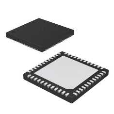
 LCMXO2-640HC-4TG100C - Brand New LATTICE Programmable Logic Device (CPLDs/FPGAs)QFP-100
 -
 LC4032V-75TN48C - Brand New Lattice Semiconductor Programmable Logic Device (CPLDs/FPGAs)48-LQFP
 -
 EPM3128ATC144-10N - Brand New Intel / Altera Programmable Logic Device (CPLDs/FPGAs)QFP
 -
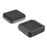 XC9572-7PC44C - Brand New XILINX Programmable Logic Device (CPLDs/FPGAs)44-LCC J-Lead
 -
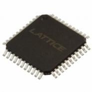 M4A3-32/32-10VC - Brand New Lattice Semiconductor Programmable Logic Device (CPLDs/FPGAs)44-TQFP
 -
 EPM3032ATC44-10N - Brand New Intel / Altera Programmable Logic Device (CPLDs/FPGAs)QFP-44
 -
LCMXO1200C-3FTN256C - Brand New Lattice Semiconductor Programmable Logic Device (CPLDs/FPGAs)256-LBGA
-
 EPM7256SRI208-10N - Brand New Intel / Altera Programmable Logic Device (CPLDs/FPGAs)QFP
 -
 XC9572XL-10TQ100I - Brand New XILINX Programmable Logic Device (CPLDs/FPGAs)TQFP
 -
 EPM1270T144I5N - Brand New Intel / Altera Programmable Logic Device (CPLDs/FPGAs)144-LQFP
-
The fee is charged according to the rule of PayPal.
-
The fee is charged according to the rule of PayPal.
-
Western Union charge US$0.00 banking fee.
-
We recommend to use bank transfer for large orders to save on handling fees.
-
DHL(www.dhl.com)
$40 limited time offer. -
UPS(www.ups.com)
$40 limited time offer. -
FedEx(www.fedex.com)
$40 limited time offer. -
Registered Mail(www.singpost.com)
Free shipping without minimum order.
