⚠ All product names, trademarks, brands, and logos on this site are the property of their respective owners. Their use is for identification purposes only and does not imply any affiliation or authorization from the rights holders. We are not authorized dealers or distributors of the brand. The warranty is provided by us, not the original manufacturer.
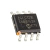
TE28F128J3D75
TE28F128J3D75 - Brand New Intel Memory


 Credit Card
 - One-month free return and one year warranty.
- Full or Partial Refund, if the item is not as described
- Full Refund if you don't receive your order
Description
The Numonyx™ Embedded Flash Memory (J3 v D) device includes new security features that were not available on the (previous) 0.25µm and 0.18µm versions of the J3 family. These new security features prevent altering of code through different protection schemes that can be implemented, based on user requirements.
The Numonyx™ Embedded Flash Memory (J3 v D, Monolithic) optimized architecture and interface dramatically increases read performance by supporting page-mode reads. This read mode is ideal for non-clock memory systems.
Its Common Flash Interface (CFI) permits software algorithms to be used for entire families of devices. This allows device-independent, JEDEC ID- independent, and forward- and backward-compatible software support for the specified flash device families. Flash vendors can standardize their existing interfaces for long-term compatibility.
The Scalable Command Set (SCS) allows a single, simple software driver in all host systems to work with all SCS-compliant flash memory devices, independent of systemlevel packaging (e.g., memory card, SIMM, or direct-to-board placement). Additionally, SCS provides the highest system/device data transfer rates and minimizes device and system-level implementation costs.
A Command User Interface (CUI) serves as the interface between the system processor and internal operation of the device. A valid command sequence written to the CUI initiates device automation. An internal Write State Machine (WSM) automatically executes the algorithms and timings necessary for block erase, program, and lock-bit configuration operations.
A block erase operation erases one of the device’s 128-Kbyte blocks typically within one second, independent of other blocks. Each block can be independently erased 100,000 times. Block erase suspend mode allows system software to suspend block erase to read or program data from any other block. Similarly, program suspend allows system software to suspend programming (byte/word program and write-to-buffer operations) to read data or execute code from any other block that is not being suspended.
Each device incorporates a Write Buffer of 32 bytes (16 words) to allow optimum programming performance. By using the Write Buffer data is programmed more efficiently in buffer increments.
Features
■ Architecture
— Symmetrical 128-Kbyte blocks
— 256 Mbit (256 blocks)
— 128 Mbit (128 blocks)
— 64 Mbit (64 blocks)
— 32 Mbit (32 blocks)
■ Performance
— 75 ns Initial Access Speed (32,64,128 Mbit densities)
— 95 ns Initial Access Speed (256Mbit only)
— 25 ns 8-word and 4-word Asynchronous page-mode reads
— 32-Byte Write buffer; 4 µs per Byte Effective programming time
■ System Voltage
— VCC = 2.7 V to 3.6 V
— VCCQ = 2.7 V to 3.6 V
■ Packaging
— 56-Lead TSOP (32, 64, 128, 256 Mbit)
— 64-Ball Numonyx Easy BGA package (32, 64, 128 and 256 Mbit)
■ Security
— Enhanced security options for code protection
— 128-bit Protection Register: 64-bits Unique device identifier bits 64-bits
User-programmable OTP bits
— Absolute protection with VPEN = GND
— Individual block locking
— Block erase/program lockout during power transitions
■ Software
— Program and erase suspend support
— Flash Data Integrator (FDI), Common Flash Interface (CFI) Compatible
■ Quality and Reliability
— Operating temperature: -40 °C to +85 °C
— 100K Minimum erase cycles per block
— 0.13 µm ETOX™ VIII Process technology
Shipping
| First item | Additional item | Service | Description |
|---|---|---|---|
| $0.00 | Free | Free Shipping | Estimated 15-30 business days via Registered Air Mail or others |
| $27.50 | Free | Expedited Shipping | Estimated delivery time is 3-5 business days, with some areas possibly taking 6-9 business days depending on the shipping address. The main courier companies include but are not limited to UPS, DHL, and FedEx. |
| $0.00 | Free | Buyer cooperating carrier | Using buyer's cooperating carrier. Buyer should create a shipping label and share it to us. And then we will call carrier for pickup |
| $38.00 | Free | Expedited Shipping | Estimated delivery time is 3-5 business days, with some areas possibly taking 6-9 business days depending on the shipping address. The main courier companies include but are not limited to UPS, DHL, and FedEx. |
Delivery
- The transportation time may be delayed due to customs clearance, local holidays or abnormal events.
- The estimated time is based on the fastest speed provided by commercial couriers (DHL, FedEx, UPS etc).
- The estimated time does not include the lead time of the item. The lead time of most items is 2–5 business days. If more than 5 working days are needed, we will manually confirm with you.
| Flag | Country | Express Delivery | Standard Delivery |
|---|---|---|---|
 | United States | 3 - 5 days | 10-15 days |
 | Canada | 3 - 5 days | 10-20 days |
 | Mexico | 3 - 5 days | 10-17 days |
 | Germany | 3 - 5 days | 10-12 days |
 | Italy | 3 - 5 days | 10-15 days |
 | United Kingdom | 3 - 5 days | 10-12 days |
Estimated Delivery
This item requires 2-5 business days for processing before shipping after payment is confirmed. And depending on the destination and shipping method.
Return Policy
| Return window | Refund type | Return shipping |
|---|---|---|
| 60 days after receiving item | Money Back or Replacement | Buyer pays for return shipping |
Verified buyer reviews for electronic components and industrial control products.
 In Stock
 23K256-I/SN
23K256-I/SN - Brand New Microchip Technology Memory
 In Stock
 24AA025E48T-I/OT
24AA025E48T-I/OT - Brand New Microchip Technology Memory
 In Stock
 24AA02T-I/OT
24AA02T-I/OT - Brand New Microchip Technology Memory
 In Stock
 24AA64-I/MS
24AA64-I/MS - Brand New Microchip Technology Memory
 In Stock
 24AA64-I/SN
24AA64-I/SN - Brand New Microchip Technology Memory
 In Stock
 24AA64T-I/MS
24AA64T-I/MS - Brand New Microchip Technology Memory
 In Stock
 24AA64T-I/OT
24AA64T-I/OT - Brand New Microchip Technology Memory
 In Stock
 24FC256-I/SN
24FC256-I/SN - Brand New Microchip Technology Memory
 In Stock
 24LC128-I/ST
24LC128-I/ST - Brand New Microchip Technology Memory
 In Stock
 24lc128t-i/sn
24lc128t-i/sn - Microchip - Technology Memory